By clicking “Accept All Cookies”, you agree to the storing of cookies on your device to enhance site navigation, analyze site usage, and assist in our marketing efforts. View our Privacy Policy for more information.
Background moutain Attolight
Allalin

Hybridized SEM – Spectroscopic Platform

  • SEM – Quantitative Cathodoluminescence (qCL)
  • Spectroscopic Analysis (Photoluminescence, Raman, …)
  • Time-resolved measurements (TRCL, TRPL, g², …)
  • Electrical Measurements (EBIC/EBAC)
  • Room to low-temperature analyses (<10K)
  • Cryo-compatible Nanoprobes
Dashboard mockup
Characteristics

About our Hybridized SEM – Spectroscopic Platform

The Allalin is a nanometer-resolution SEM-spectroscopic instrument featuring a unique optical collection objective integrated within the SEM column, which allows for robust and repeatable measurements, enabling quantitative cathodoluminescence (qCL) analysis.

One Platform, Multiple Measurement Possibilities

The Allalin platform supports a wide range of spectroscopic analysis techniques, utilizing multiple sources (electron beam or laser, in continuous or pulsed mode) and various detectors (SE detector, PMT, CCD/Streak cameras, InGaAs/TCSPC/HPD detectors).

The system can also be equipped with options like in-SEM electrical probing, Raman spectroscopy, Photoluminescence, and HBT setup for g(2) autocorrelation measurement.

Different stage options are available to accommodate samples as small as a few micrometers to wafers up to 6 inches.

Finally, spectroscopic analyses can be conducted at temperatures ranging from 10 K to 320 K, thanks to an integrated helium cryostat and a unique hexapod-based stage design, which ensures high stability and very low drift (<5 nm/min).

Dashboard mockup

Trusted by top semiconductor companies and prestigious research institutes worldwide

Applications

Related Applications Using the Allalin Platform

Discover how the Allalin platform can support your research.

Text Link
Process development
Text Link
Materials Science
Text Link
Micro/Nanowire
Text Link
GaN device
Text Link
Power electronics
Text Link
Life Science
Text Link
Optoelectronics
Text Link
Application

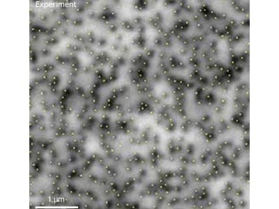
Applications on Defect Visualization and Counting in Optoelectronic Materials

Find out how CL can quantify defects in optoelectronic materials
Text Link
Application

Applications on Semiconducting Diamond

Find out how CL can investigate semiconducting properties of diamond
Text Link
Application

Applications on Photovoltaic Materials

Find out how CL can investigate QD nanowires
Text Link
Application

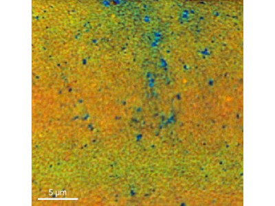
Applications on Hyperspectral Mapping with high Spatial Resolution for Optoelectronic Devices

Find out how CL can defect defects in optoelectronic materials
Text Link
Application

Applications on GaN for Power Electronic

Find out how CL can investigate QD nanowires
Text Link
Application

Applications on ZnO micro/nanowire Materials

Find out how CL can investigate QD nanowires
Text Link
Application

Pinhole Detection in Photovoltaic and Thin Film Battery Materials

Find out how CL helps to improve device performances
Text Link
Application

Applications on Quantum Heterostructures

Find out how CL can investigate QD nanowires
Text Link
Application

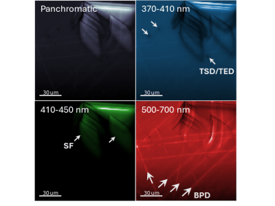
Comprehensive defect review and classification for SiC

We show how spectrally-resolved quantitative CL can be used to classify various defects in SiC
Text Link
Application

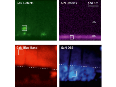
Non-destructive control of epitaxial layer uniformity in GaN power devices

We will show how spectrally-resolved quantitative CL can address this challenge

Scientific references

Influence of Shape and Size on GaN/InGaN μLED Light Emission: A Competition between Sidewall Defects and Light Extraction Efficiency GONZÁLEZ-IZQUIERDO, Palmerina, ROCHAT, Névine, ZOCCARATO, Davide, et al. ACS Photonics, 2023 2023
Enriching the Deep-Red Emission in (Mg, Ba)3M2GeO8: Mn4+ (M= Al, Ga) Compositions for Light-Emitting Diodes KURUNTHATIL KUTTIAT, Thejas, ABRAHAM, Malini, KUNTI, Arup K., et al. ACS Applied Materials & Interfaces, 2023 2023
Epitaxial lateral overgrowth of GaN on a laser-patterned graphene mask KADYS, Arūnas, MICKEVIČIUS, Jūras, BADOKAS, Kazimieras, et al. Nanomaterials, 2023, vol. 13, no 4, p. 784 2023
Dynamics of double-peak photoluminescence in m-plane InGaN/GaN MQWs MICKEVIČIUS, J., VALKIŪNAITĖ, E., PODLIPSKAS, Ž., et al. Journal of Luminescence, 2023, p. 119732 2023

Scientific references

Role of Compositional Fluctuations and Their Suppression on the Strain and Luminescence of InGaN Alloys PANTZAS, K., PATRIARCHE, G., TROADEC, D., KOCIACK, M., CHERKASHIN, N., HÿTCH, M., BARJON, J., TANGUY, C., RIVERA, T., SURESH, S., OUGAZZADEN, A. Journal of Applied Physics, 2015, 117, 055705 2015
Mapping Plasmons at the Nanometer Scale in an Electron Microscope KOCIACK, M., STÉPHAN, O. Chemical Society Reviews, 2014, 43, 3865–3883 2014
Nanometric Resolved Luminescence in h-BN Flakes: Excitons and Stacking Order BOURRELLIER, R., AMATO, M., TIZEI, L. H. G., GIORGETTI, C., GLOTER, A., HEGGIE, M. I., MARCH, K., STÉPHAN, O., REINING, L., KOCIACK, M., ZOBELLI, A. ACS Photonics, 2014, 1, 857 2014
Seeing and Measuring in Colours: Electron Microscopy and Spectroscopies Applied to Nano-optics KOCIACK, M., STÉPHAN, O., GLOTER, A., ZAGONEL, L. F., TIZEI, L. H. G., TENCÉ, M., MARCH, K., BLAZIT, J. D., MAHFOUD, Z., LOSQUIN, A., MEURET, S., COLLIEX, C. Comptes Rendus Physique, 2014, 15, 158–175 2014

Ready to revolutionize your materials characterization approach?

Get in touch with us today to discover how our state-of-the-art cathodoluminescence tools can elevate your research and industry applications.
Already more than 30 systems installed globally!