Comprehensive Defect Review and Classification for SiC
SiC films are inherently defective due to their complicated fabrication process and polytypic nature. The current approach to quality control involves defect mapping by photoluminescence (PL). This approach, however, cannot reliably identify defect subclass, which has a profound effect on downstream yield, performance and reliability. In this application note, we introduce cathodoluminescence (CL) hyperspectral mapping as a complementary metrology technique which can better classify defects in SiC. Attolight’s approach enables high-throughput defect review for unprecedented insights for SiC power electronics and beyond.
SiC substrate fabrication and subsequent epitaxial processes are susceptible to various crystal defects. Different defect types have different effects on device performance, many of which lead to yield loss or premature device failure. Thus, SiC layers should be carefully inspected and characterized in order to ensure maximum yield and reliability for power electronics products.
Traditionally, photoluminescence (PL) scanners are used for SiC substrate inspection. The result of this process is a wafer map that includes information about the shape of defects and whether they are dark or bright. However, defect shape is not always correlated to defect type, and PL is not able to identify stacking fault or threading dislocation subclasses, which can have varying impacts on yield and reliability. Additionally, at typical PL wavelengths, the laser penetrates far beyond the epitaxial layer of SiC, probing mostly the substrate.
Cathodoluminescence (CL) is an ideal approach to classifying and quantifying defects, including subclasses, thanks to its high-energy excitation and its excellent spatial and spectral resolution. The acquisition of hyperspectral maps allows one to image a large field of view (FOV) and classify the defects present thanks to their unique spectral signature.
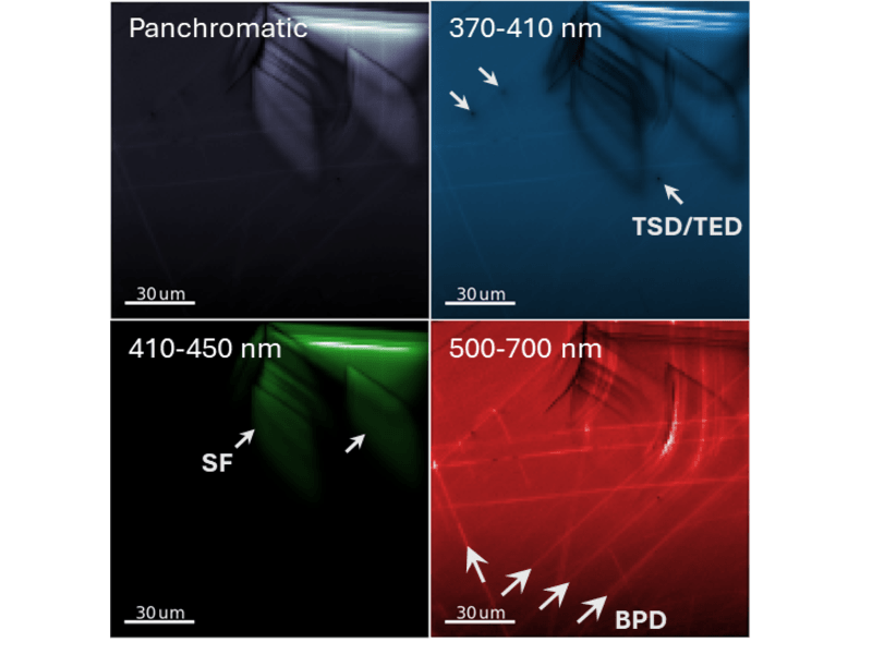
Figure 1 shows an example of the power of hyperspectral imaging to visualize and classify defects present in SiC films. Contrast in the panchromatic map, which shows the integrated emission intensity over the full spectral range, indicates the presence of various crystallographic features that can be further resolved by looking at specific bands within the emission spectra. The blue image corresponds to 4H-SiC near band edge emission (NBE, 370 – 410 nm), where we can see the presence of threading dislocations (threading screw dislocations, TSDs, or threading edge dislocations, TEDs) as dark spots where emission is quenched. The green image corresponds to emission from stacking faults (SFs), which have a smaller band gap energy and act as quantum wells (QWs) in the SiC lattice. This QW behavior favors recombination in the SF and gives rise to the most intense component of the emission spectrum. Finally, the red image corresponds to donor-acceptor pair (DAP) emission, allowing one to visualize basal plane dislocations (BPDs) as bright lines due to accumulation of donor and acceptor impurities at these kinds of defects.
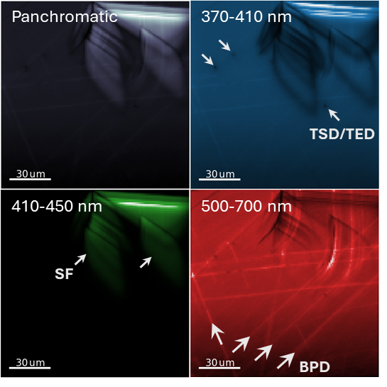
Interestingly, many of these defects can be further sub-classified depending on their emission characteristics. For example, there are several kinds of SFs which occur in 4H-SiC, each of which has a unique emission wavelength. The SFs shown in Figure 1 correspond to single Shockley SFs, which emit around 425 nm, whereas triple Shockley SFs would emit around 480 nm. Since different kinds of SFs are believed to have different impacts on ultimate device performance and reliability, Attolight’s approach to quantitative CL is a powerful tool for understanding the impact of SFs on SiC devices.
Threading dislocations (TDs) can also be sub-classified based on their CL signature. Specifically, edge and mixed-type dislocations result in non-centrosymmetric strain, giving rise to a dipole-like peak shift around the dislocation center. This is illustrated in Figure 2, where the NBE amplitude and peak shift is shown for two dislocations, each exhibiting edge-like signatures.
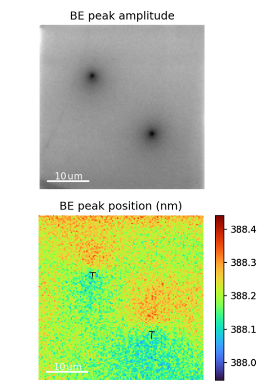
Screw-type dislocations, on the other hand, exhibit no such dipole-like behavior. This means that hyperspectral maps containing TDs can be analyzed to distinguish TEDs from TSDs, a feat which is impossible with PL due to its lower spatial resolution. Similar analysis is possible in other materials systems, such as GaN, and can also be further classified in CL using degree of polarization (DOP) measurements. In this way, the Attolight CL platform enables advanced classification of various SiC defects beyond the capabilities of PL.
The analysis presented here relies on the use of CL hyperspectral maps, which generally take tens of seconds to acquire, depending on resolution. This makes CL an ideal complement to PL scanning; CL can be used to review a subset of defects that are identified by the relatively fast PL process. The defect map and initial classification data is simply fed-forward to the CL tool, which then drives to the appropriate location on the wafer to perform a detailed review of the defects of interest.
Thanks to their large FOV and rapid, reliable optical alignment procedure, Attolight CL systems are able to quickly measure multiple defect locations on a wafer. This offers a new path toward process control and development for SiC, giving unprecedented insight into the origin and effects of ubiquitous defects present from the epitaxial growth process. Hyperspectral CL imaging moves beyond the capabilities of current metrology techniques for classification of defect type, all while maintaining industrial-scale throughput.



.webp)
