By clicking “Accept All Cookies”, you agree to the storing of cookies on your device to enhance site navigation, analyze site usage, and assist in our marketing efforts. View our Privacy Policy for more information.

CL from beam-sensitive optoelectronic materials - hybrid halide perovskites

Find out how CL quantify defects in optoelectronic materials
Abstract

Halide perovskites have emerged as exceptional candidates for next-generation optoelectronic applications such as solar cells and light emission diodes. Perovskite thin films are heterogeneous at the micro- and nano- length scales in their structure and properties. The understanding of the nanoscale is fundamental for the development and improvement of these novel materials. CL allows the properties of the material to be probed at a high spatial resolution. However, these soft semiconductors are highly sensitive to electron beam damage, which has majorly hindered the use of CL.

Spatially resolved CL maps against lowering beam current, exhibiting more robust emission. CW: Continuous-wave and PM: pulsed-mode electron beam acquisition.

The use of pulsed mode scanning electron microscopy cathodoluminescence (PM SEM-CL) has been found to be useful for the study of hybrid perovskite films. These findings were enabled by the Attolight Allalin setup.

The use of a pulsed beam enables the imaging of the heterogeneity of the emission properties of hybrid perovskite films at the nanoscale via the acquisition of CL hyperspectral maps due to the low-dose pulsed nature of the electron beam.

These optimized parameters also enable the acquisition of time-resolved CL of polycrystalline films, showing significantly

shorter lived charge carriers dynamics compared to the photoluminescence analogue, which suggest electron beam-specimen interactions attributed to beam damage.

These findings represent a promising step to unlock the use of CL hyperspectral mapping and TRCL on the more beam-sensitive hybrid perovskite compositions. In extension, we anticipate that CL in low-dose regimes will play a large role in resolving the complex nanoscale of other organic and beam-sensitive semiconductors.

See more details in https://doi.org/10.1088/2632-959X/abfe3c

References
Published on
November 5, 2024
Discover our products used to realize this application
No items found.
Applications

More applications

Text Link
Power Electronics
Text Link
Quantum technologies
Text Link
Sensors
Text Link
Life sciences
Text Link
Energy Materials
Text Link
RF / power transistors
Text Link
Optoeletronics
Text Link
Application

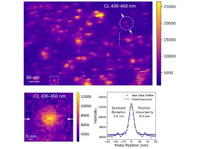
Applications on Defect Visualization and Counting in Optoelectronic Materials

Find out how CL can quantify defects in optoelectronic materials
Text Link
Application

Applications on Semiconducting Diamond

Find out how CL can investigate semiconducting properties of diamond
Text Link
Application

Applications on Photovoltaic Materials

Find out how CL can investigate QD nanowires
Text Link
Application

Applications on Hyperspectral Mapping with high Spatial Resolution for Optoelectronic Devices

Find out how CL can defect defects in optoelectronic materials
Text Link
Application

Applications on GaN for Power Electronic

Find out how CL can investigate QD nanowires
Text Link
Application

Applications on ZnO micro/nanowire Materials

Find out how CL can investigate QD nanowires

Ready to revolutionize your materials characterization approach?

Get in touch with us today to discover how our state-of-the-art cathodoluminescence tools can elevate your research and industry applications.
Already more than 30 systems installed globally!