
Quantitative Cathodoluminescence
.webp)
Introduction
Quantitative cathodoluminescence (q-CL) is a technique pioneered by Attolight, derived from regular cathodoluminescence. It involves the use of a reflective objective instead of off-axis parabolic mirrors or other non-imaging optics to collect luminescence signal from samples. The objective is aberration corrected and its optical axis is colinear with the scanning electron beam. Not only does this eliminate intensity and resolution artefacts during CL data acquisition, but also makes tool alignment significantly faster and enables high efficiency CL mappings over much larger areas than using regular add-on technologies.
Principles
Using aberration-corrected collection optics enables one key advantage: Cathodoluminescence imaging over a large field of view, without degradation of the system’s optical performance (off-axis aberrations) or collection efficiency (vignetting).

Figure 1 shows simulation of image spot sizes produced by typical CL-SEM configurations: Attolight’s aberration-corrected CL objective or a parabolic mirror. Image formation is considered in both cases by focusing with an achromatic lens, which is commonly used to couple signals into a spectrograph. The horizontal line denotes limitation induced by the pixel size of a typical spectroscopy CCD camera. While a parabolic mirror offers diffraction-limited performance at the very center of its field of view, its image spot size increases rapidly away from its optical axis. An aberration-corrected objective, on the other hand, presents only minor spot size variation even at significant distances from its focal axis. Quickly, spot sizes generated by Attolight’s aberration-corrected technology offer more than an order of magnitude improvement over parabolic mirrors. This also makes sure that collection performance is maintained over large CL imaging areas. In comparison, parabolic mirrors lose coupling efficiency (to fibers or through the spectrometer slit), spectral resolution, or both.
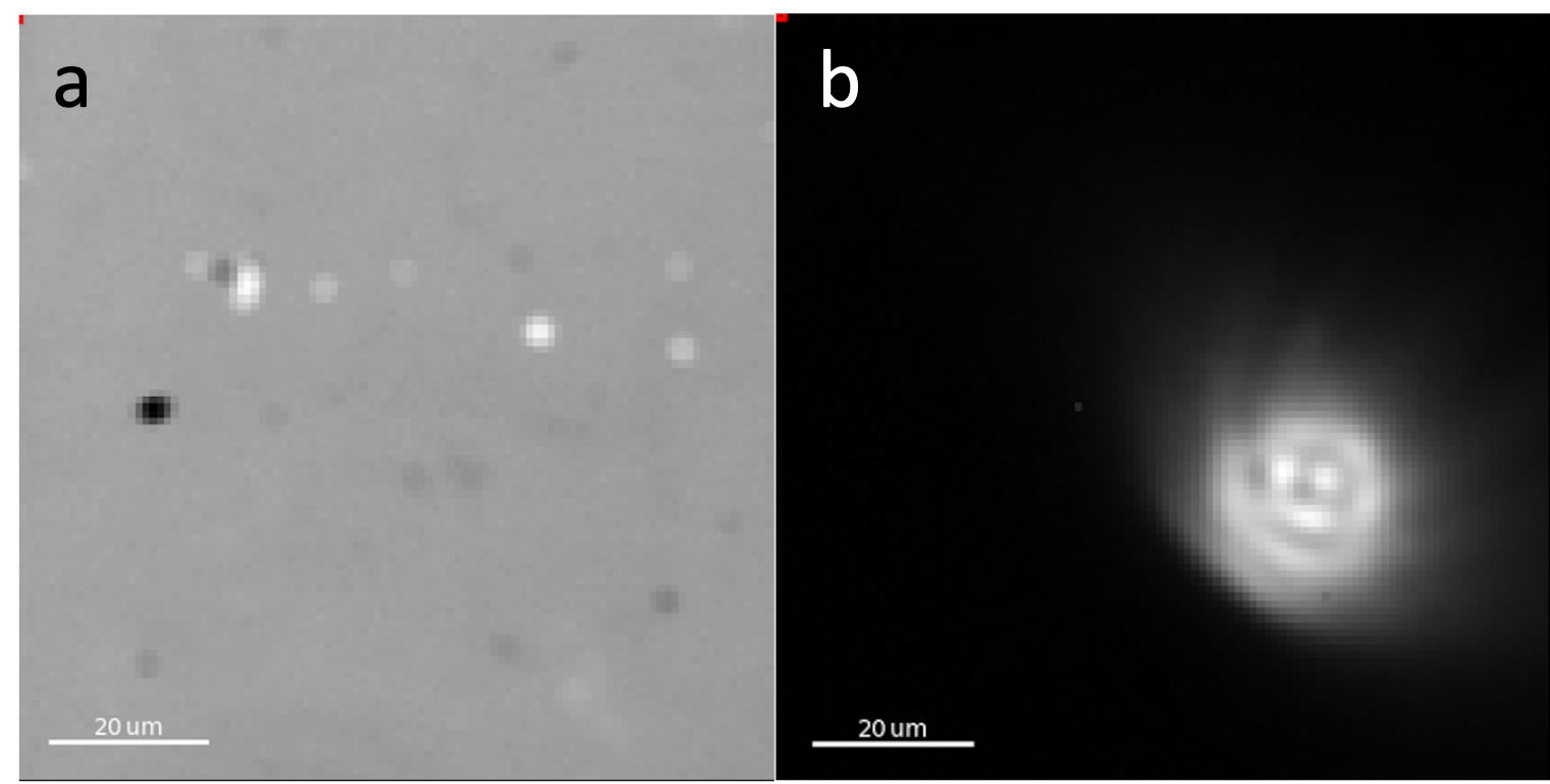
The large-surface light collection capability of Attolight’s optical system eliminates the need for adding a lateral alignment system to position the optics with respect to the electron beam. This also means that the system can record large-field-of-view (100’s of µm) maps with constant collection efficiency, thus becoming truly quantitative. Figure 2 shows an actual example of data recorded using both q-CL and parabolic-mirror CL detection systems on the same field of view of the same sample (a piece of Nd:YAG showing bright, homogeneous emission). The parabolic system has a significantly reduced effective collection area and exhibits coupling efficiency artefacts due to coupling into a fibre bundle, used here to enhance collection efficiency. These artefacts result in an inhomogeneous signal that makes it impossible to quantitatively compare the luminescence from even a small region of the sample. While in principle it would be possible to improve the homogeneity by defocusing the parabolic mirror, this would come at the cost of a significant reduction in signal intensity and spatial resolution.
Instrumentation
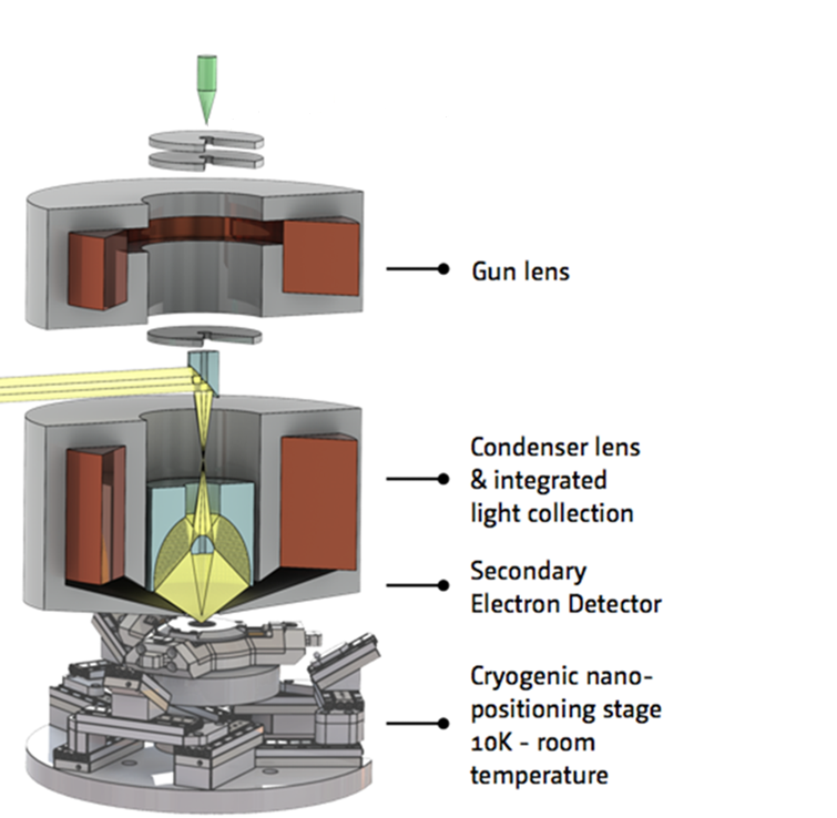
Figure 3 shows an example implementation of a q-CL apparatus. To make the mechanical integration possible, the mirror is not a free-standing add on, but is integrated coaxially with the electron microscope column, meaning that the mirror is factory aligned once and doesn’t need further care.
Example results
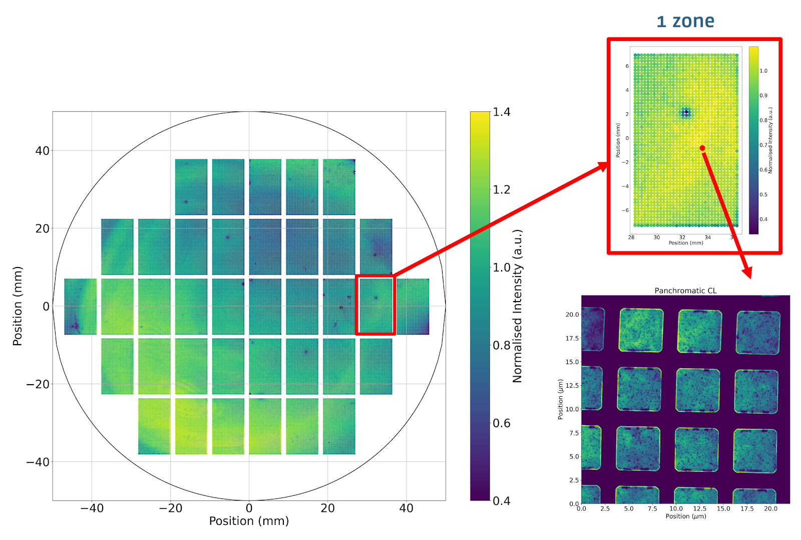
Figure 4 shows a full wafer map of microLED array intensity measurements using q-CL. q-CL makes comparison possible within each device, between devices, as well as between regions across the full surface of the wafer. Such reliable, quantitative comparison is invaluable to identify process variations and potential failures. This allows for a smooth bridging between nm- and mm-scale properties of the devices, and allows for efficient characterization of deposition process homogeneity, as well as lithography process quality and fundamental emission properties of the devices.
Benefits and Further Reading
Over the years, q-CL has benefited many users in their scientific and industrial endeavours. Check the publication page of our website to stay up to date with the latest applications. Here are two selected, free-to-read scientific publications highlighting the benefits of q-CL. In [1], luminescence properties of a polycrystalline material are compared over large areas. In reference [2], q-CL is used to identify defect densities and light-emitting quantum dots over large areas of an epitaxial sample.
References
- [1] J. Moseley et al., “Luminescence methodology to determine grain-boundary , grain-interior , and surface recombination in thin-film solar cells,” J. Appl. Phys., vol. 124, no. 113104, pp. 1–13, 2018.
- [2] J. Selvidge, J. Norman, E. T. Hughes, J. Selvidge, J. Norman, and E. T. Hughes, “Defect filtering for thermal expansion induced dislocations in III – V lasers on silicon,” Appl. Phys. Lett., vol. 122101, no. July 2020, pp. 1–6, 2021.
Latest Scientific Publications
Quantitative Cathodoluminescence

Quantitative CL Uniquely Resolves Individual Point Defects in InGaN/GaN Quantum Wells, Solving Efficiency Gain Riddle
CL from Beam-Sensitive Optoelectronic Materials - Hybrid Halide Perovskites
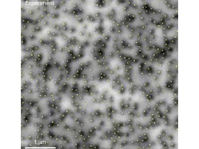
Applications on Defect Visualization and Counting in Optoelectronic Materials
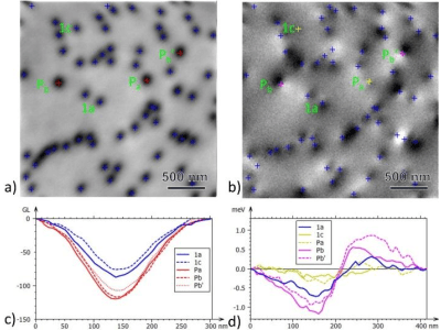
Dislocation Type Determination by Cathodoluminescence
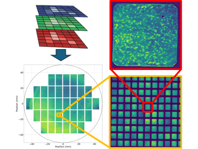
Non-Destructive Quality Control of Micron-Sized Light Emitting Diodes
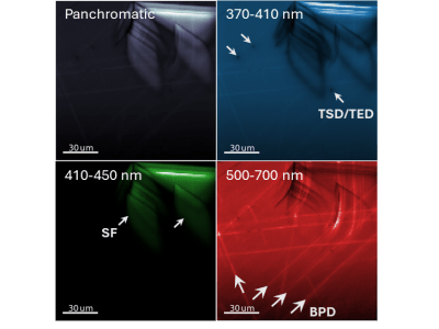
Comprehensive Defect Review and Classification for SiC
Non-Destructive Control of Epitaxial Layer Uniformity in GaN Power Devices
Explore our high-resolution cathodoluminescence tools designed for superior materials characterization.


