Non-Destructive Control of Epitaxial Layer Uniformity in GaN Power Devices
The rapid growth of the GaN-based High Electron Mobility Transistor (HEMT) market highlights the need for improved process control metrology. Traditional methods relying on destructive wafer analysis are costly, slow, and inefficient. This application note introduces quantitative cathodoluminescence (CL) as a non-destructive, in-line metrology technique for monitoring critical material properties, such as the aluminum fraction in AlGaN layers. The Attolight CL system, with its advanced optics and large-area electron beam irradiation, enables accurate detection of weak AlGaN signals, ensuring robust process control and faster tool qualification.
The market for High Electron Mobility Transistors (HEMTs) based on gallium nitride (GaN) is growing rapidly, but process control metrology has not kept up. Currently, the process control strategy for HEMT production on silicon substrates relies on the routine sacrifice of production wafers for external analysis, an approach that is costly, wasteful, and has a slow turnaround time, leaving the production line vulnerable to major excursions. Quantitative cathodoluminescence (CL) is a promising approach for non-destructive, in-line metrology of critical material properties, allowing for a tighter and more robust process control strategy and faster epi tool qualification after maintenance.
One particularly difficult parameter to control in HEMTs is the aluminum fraction of the AlGaN barrier. This layer is key to the core functionality of the transistor, but its composition is susceptible to fluctuations in precursor flow rates in the MOVPE reactor. For enhancement-mode HEMTs, the AlGaN layer is buried under a highly absorptive pGaN layer that makes probing the AlGaN layer by photoluminescence (PL) spectroscopy difficult, since the probing laser will be greatly attenuated inside the upper pGaN layer.
In contrast to PL, which generally uses a fixed wavelength laser whose penetration depth cannot be adjusted, CL uses an electron beam probe whose penetration depth can be tuned from tens to hundreds of nanometers by varying the beam energy. This allows for selective probing of different layers in the device stack.
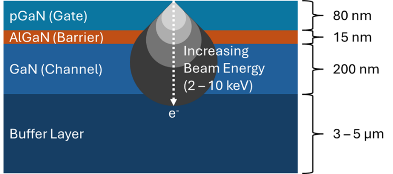
Figure 1 shows a schematic diagram of a typical GaN HEMT stack as well as the variable penetration depth of the CL electron beam probe as a function of beam energy.
To probe the AlGaN layer, an appropriate beam energy must be carefully selected. Interactions between the electron beam and the AlGaN layer result in emission of light with a characteristic wavelength, whose energy can be correlated to the bandgap energy, and thereby aluminum fraction, of the AlGaN layer. However, the amount of light originating from the AlGaN layer is small compared to the amount coming from the GaN layers that sandwich it. This is due to a combination of factors, including the small thickness of the layer and its band alignment, which favors recombination in the GaN layers above and below. What’s more, much of the light emitted from the AlGaN layer is absorbed in the pGaN top layer before it can exit the sample surface. This means that the final luminescent intensity from the AlGaN layer is weak and challenging to detect.
This is where the advanced optics of the Attolight CL system come into play. Light from the sample is collected using our proprietary objective lens, which is integrated directly into the electron column. This configuration allows for efficient light collection over a large field of view in a way that is robust to the kind of beam displacement effects that occur when changing excitation conditions. The fully integrated Attolight system can detect even extremely weak signals that otherwise would not be detectable with CL add-on systems.
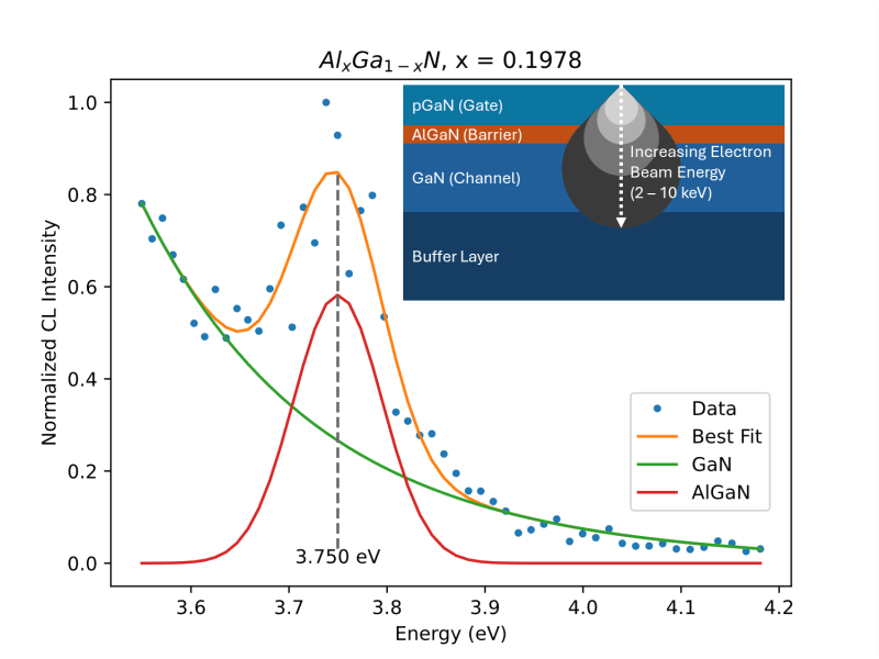
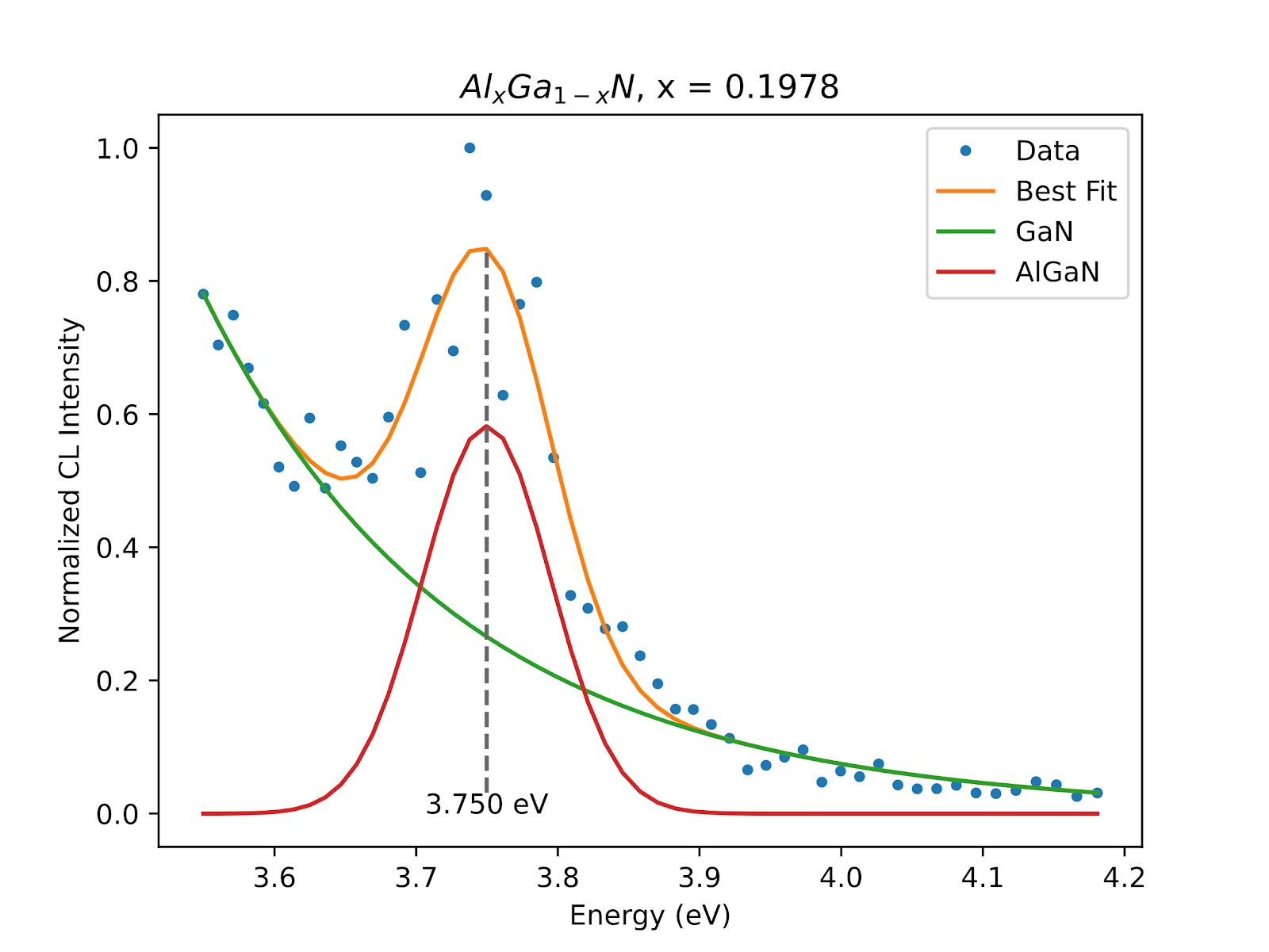
The result is that, despite the weak and attenuated AlGaN emission, the Attolight system is able to detect and fit the resulting spectra in order to reliably measure the aluminum fraction of the layer (AlxGa1-xN; x=0.2407), as shown in Figure 2.
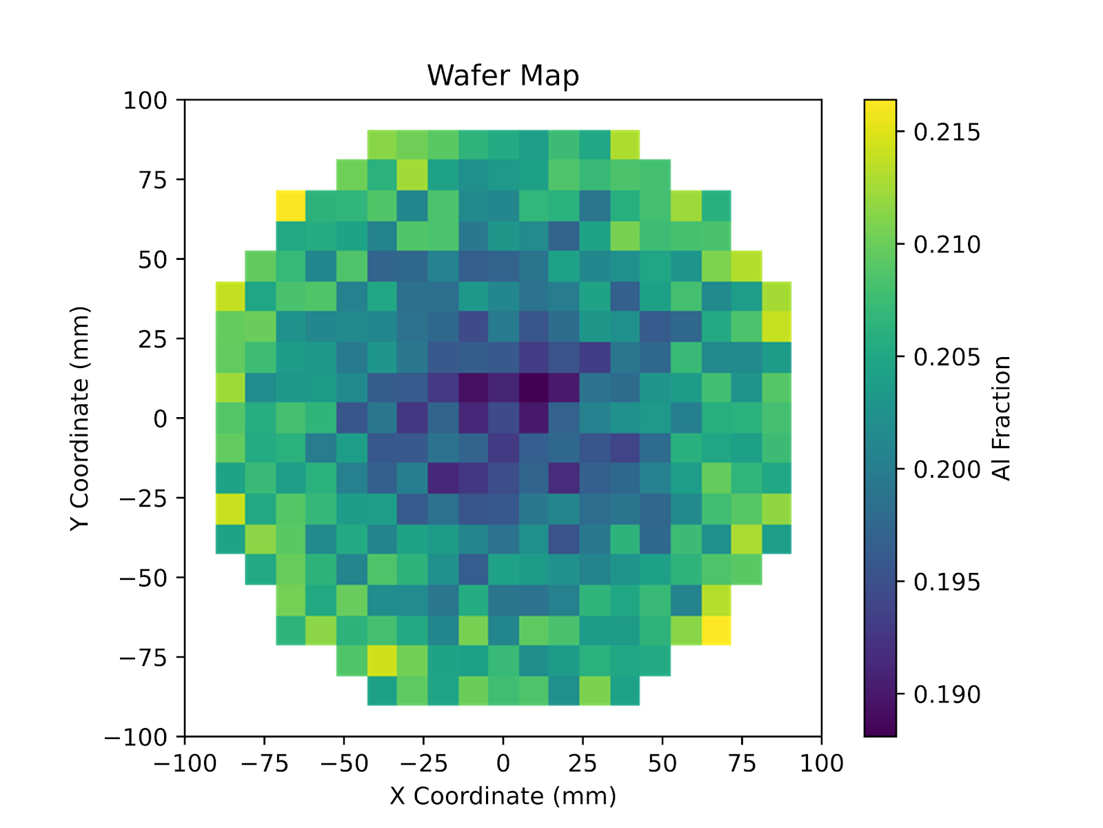
Thanks to the full-wafer capabilities of the Säntis 300, wafer-level statistics can be performed, as shown in Figure 3, as well as lot-to-lot monitoring. This ensures that process engineers have the data they need to quickly identify when their epi process goes out of control and can shut down the offending reactor, preventing costly excursions that could lead to scrap or down-binning of product.



.webp)
