State-of-the-Art Instruments for Advanced Materials Science and Semiconductor Defect Inspection

Our Advanced Product Lineup
Discover our high-performance cathodoluminescence solutions, engineered for exceptional materials characterization. Our range includes versatile multi-spectroscopic CL SEM platforms, CL STEM add-ons and automated wafer CL SEM systems, delivering unparalleled precision and adaptability to meet all your materials inspection requirements.


About Cathodoluminescence
Attolight revolutionizes cathodoluminescence analysis with its innovative optical collection design, seamlessly integrated into a SEM column. This advanced system enables precise quantitative analysis and enhances the charaterization of any materials, thanks to its highly efficient photon collection.
Elevate your research and quality control standards with Attolight’s cutting-edge technology!

Trusted by top semiconductor companies and prestigious research institutes worldwide


Innovative Applications of Cathodoluminescence Technology
Pushing the boundaries of material characterization.
Identifying Atomic-Scale Defects Responsible for Blue Emission in hBN Using Correlative STEM-CL

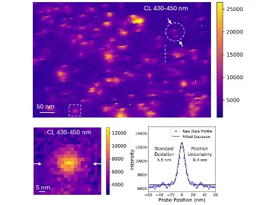
Quantitative CL Uniquely Resolves Individual Point Defects in InGaN/GaN Quantum Wells, Solving Efficiency Gain Riddle
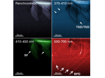
Comprehensive Defect Review and Classification for SiC
Stay informed with our latest developments and events
Stay informed with the latest developments, breakthroughs, and insights.

Meet Attolight at Microscopy & Microanalysis (M&M) 2026
.webp)
Meet Attolight at IMC21 in Liverpool, 31 August–4 September 2026
UTD and Attolight Launch New Demo Lab to Advance Wide Bandgap Semiconductor R&D
Ready to revolutionize your materials characterization approach?
Establishing Cathodoluminescence as a standard inspection method
We are committed to delivering state-of-the-art solutions that provide unparalleled precision, speed, and ease-of-use, enabling our customers to drive performance and innovation in the semiconductor industry and beyond.
By establishing cathodoluminescence as a standard characterization technique, we strive to empower researchers, manufacturers, and industry leaders worldwide.
