Light Emitting Diodes (LEDs)
Applications for LEDs are growing in different end markets such as automotive, agricultural lighting, disinfection, general lighting, etc. Manufacturers are looking for improved strategies to increase yield and performance by developing better and more complex structures.
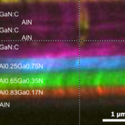
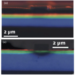
A LED structure consists of stacks of several semi-conducting layers that are grown by an epitaxial process. Quality control of each layer is crucial to ensure a highly reliable and efficient end product.
Attolight tools shorten the epitaxy development cycle through fast feedback on the quality of the epitaxial layers.
Selection of applications:
Displays
In today’s connected world, there is an ever increasing demand to show information in real time on displays. Professional users and consumers create a demand for high performance displays in various industries such as Oil & Gas, Healthcare, Manufacturing, Retail, and others. These displays need a high contrast ratio and brightness, need to be energy efficient and show long lifetimes.
An increasing number of manufacturers implement µLED and solid state laser (SSL) illumination technology within their display products.
SSL and µLED structures consist of stacks of several semi-conducting layers that are grown by an epitaxial process. Quality control of each layer is crucial to ensure a highly reliable and efficient end product.
Attolight tools shorten the epitaxy development cycle through fast feedback on the quality of the epitaxial layers.
Selection of applications:
Power & radio frequency devices
The power supply segment, new wireless charging norms, wireless communication and autonomous driving create a demand for high electron mobility transistors (HEMTs). Gallium nitride (GaN) HEMTs are a very promising technology to satisfy the needs of most of these applications. GaN HEMTs are complex combinations of strain relaxation layers and device structures grown by epitaxial processes.
Quality control of each layer is crucial to ensure a highly reliable and efficient end product.
Attolight tools shorten the epitaxy development cycle through fast feedback on the quality of the epitaxial layers.
Selection of applications:
Silicon Photonics
Silicon photonics uses light instead of electrical current to transmit information on computer chips. It is a core building block to achieve ultrafast computing.
Manufacturers are making considerable efforts in the integration of optical components onto silicon based electronic components. These optical components are grown by epitaxial processes, which is challenging due to the different structures of the materials at play as well as the significantly reduced dimensions.
Attolight tools enable these developments through high resolution quality control and fast feedback on the quality of the epitaxial layers.
Selection of applications:
Materials Characterization
A vast number of materials are being investigated and developed for future applications ranging from telecommunications to display technologies and energy production. Attolight tools have been used on a number of materials, both emerging and existing. These include silicon, 2D materials (MoS2, graphene, etc.), inorganic functional materials (perovskites, gallium oxide, zinc oxide, etc.), III-V semiconductors (gallium nitride, gallium arsenide, indium phosphide, boron nitride, etc.), and II-VI semiconductors (zinc oxide, cadmium telluride, etc.). Also, CL on biological materials is a field of increasing activity due to the high spatial resolution achieved with Attolight technology and solutions.
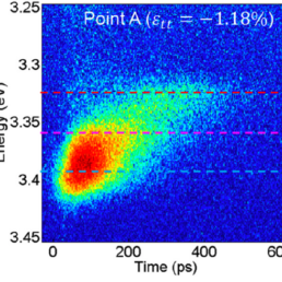
Attolight tools help researchers tackle tasks such as measuring fundamental optical end electrical properties, establishing structure-properties relationships. determining defects nature and densities. All these tasks are performed at scale from a few nm to 1 mm with an unprecedented ease-of-use, giving materials scientists maximum flexibility and efficiency to refine synthesis processes or assess new materials for example.
Selection of applications:
Defect Detection and characterization
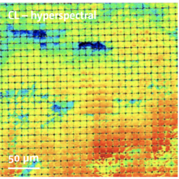
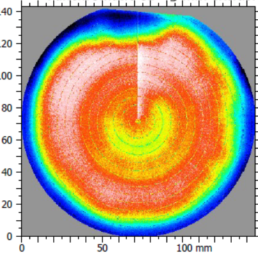
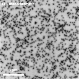
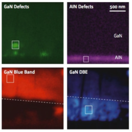
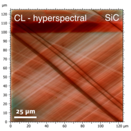
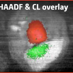
Defects locally change the crystal structure. Such change influences the wavelength and intensity of the CL signal. This makes CL is an appealing method for non-destructive high resolution defect detection and characterization.
Defect Detection and characterization
Defects locally change the crystal structure. Such change influences the wavelength and intensity of the CL signal. This makes CL is an appealing method for non-destructive high resolution defect detection and characterization.
Defect Detection and characterization
Defects locally change the crystal structure. Such change influences the wavelength and intensity of the CL signal. This makes CL is an appealing method for non-destructive high resolution defect detection and characterization.
Defect Detection and characterization
Defects locally change the crystal structure. Such change influences the wavelength and intensity of the CL signal. This makes CL is an appealing method for non-destructive high resolution defect detection and characterization.
Defect Detection and characterization
Defects locally change the crystal structure. Such change influences the wavelength and intensity of the CL signal. This makes CL is an appealing method for non-destructive high resolution defect detection and characterization.
Defect Detection and characterization
Defects locally change the crystal structure. Such change influences the wavelength and intensity of the CL signal. This makes CL is an appealing method for non-destructive high resolution defect detection and characterization.
Defect Detection and characterization
Defects locally change the crystal structure. Such change influences the wavelength and intensity of the CL signal. This makes CL is an appealing method for non-destructive high resolution defect detection and characterization.
Defect Detection and characterization
Defects locally change the crystal structure. Such change influences the wavelength and intensity of the CL signal. This makes CL is an appealing method for non-destructive high resolution defect detection and characterization.
