Hybridized SEM – Spectroscopic Platform
- SEM – Quantitative Cathodoluminescence (qCL)
- Spectroscopic Analysis (Photoluminescence, Raman, …)
- Time-resolved measurements (TRCL, TRPL, g², …)
- Electrical Measurements (EBIC/EBAC)
- Room to low-temperature analyses (<10K)
- Cryo-compatible Nanoprobes

About our Hybridized SEM – Spectroscopic Platform
The Allalin is a nanometer-resolution SEM-spectroscopic instrument featuring a unique optical collection objective integrated within the SEM column, which allows for robust and repeatable measurements, enabling quantitative cathodoluminescence (qCL) analysis.
One Platform, Multiple Measurement Possibilities
The Allalin platform supports a wide range of spectroscopic analysis techniques, utilizing multiple sources (electron beam or laser, in continuous or pulsed mode) and various detectors (SE detector, PMT, CCD/Streak cameras, InGaAs/TCSPC/HPD detectors).
The system can also be equipped with options like in-SEM electrical probing, Raman spectroscopy, Photoluminescence, and HBT setup for g(2) autocorrelation measurement.
Different stage options are available to accommodate samples as small as a few micrometers to wafers up to 6 inches.
Finally, spectroscopic analyses can be conducted at temperatures ranging from 10 K to 320 K, thanks to an integrated helium cryostat and a unique hexapod-based stage design, which ensures high stability and very low drift (<5 nm/min).

Explore Allalin Platform Options

Explore the versatility of the Allalin platform with its extensive range of customizable options.
Select your options according to your needs :
Trusted by top semiconductor companies and prestigious research institutes worldwide


Related Applications Using the Allalin Platform
Discover how an Attolight system can support your research.

Quantitative CL Uniquely Resolves Individual Point Defects in InGaN/GaN Quantum Wells, Solving Efficiency Gain Riddle
Comprehensive Defect Review and Classification for SiC
Dislocation Type Determination by Cathodoluminescence
Non-Destructive Control of Epitaxial Layer Uniformity in GaN Power Devices
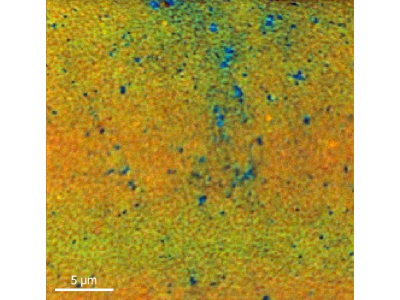
Applications on Hyperspectral Mapping with High Spatial Resolution for Optoelectronic Devices

Applications on GaN for Power Electronics
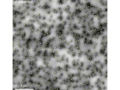
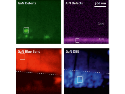
Applications on Defect Visualization and Counting in Optoelectronic Materials
.webp)
Cathodoluminescence Analysis of Extra-Cellular Matrix
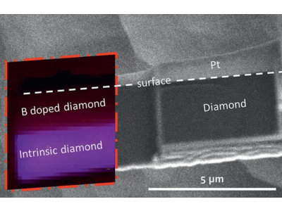
Applications on Semiconducting Diamond

Applications on Photovoltaic Materials

Applications on ZnO Micro/Nanowire Materials
Pinhole Detection in Photovoltaic and Thin Film Battery Materials
