Applications on ZnO Micro/Nanowire Materials

Due to the extraordinary properties of ZnO such as the wide direct band gap (3,37 eV), the large exciton binding energy (60 meV), and its superior optical, piezoelectric and photoelectric properties, more and more fields of applications recognize the benefits provided by this material.
Particularly in applications involving semiconducting, piezoelectric, photoelectric and high flexible mechanical properties at micro and nanoscale, ZnO micro/ nanowires are often the material of choice in numerous fields including:
- Ultraviolet lasers, detectors and photodiodes: based on the wide direct band gap and large exciton binding energy of ZnO at room temperature.
- Solar cells: ZnO micro/nanowires have large absorption window of sunlight and doping is an effective method to tune the wide band gap.
- Nano-generators: due to the strong coupling property between semiconducting and piezoelectricity of ZnO micro/nanowires.
- Electro-chemical applications: biological and chemical sensors. Optical and mechanical applications: waveguiders, strain and nanoforce sensors.

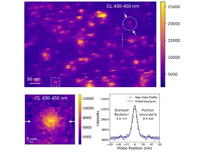
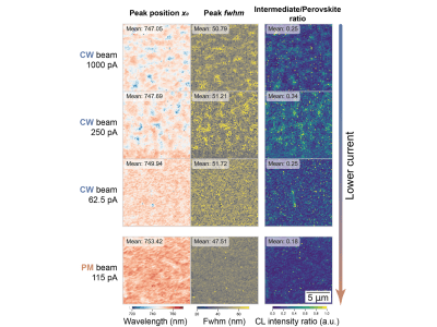
Cathodoluminescence is a key technique to study the electronic band structures of semiconductors. Its application field includes the analysis of the defect distribution, carrier dynamics and characterization of the energy band structures, all these parameters being critical to improve the design of high performance optical and electronic devices. The features of the Attolight CL system lead to a new field of research:
- Full characterization of nanostructures: with up to 10nm of spatial resolution, it is one of the most powerful tools to study local and non-local strain effects on the energy bands of ZnO micro/nanowires.
- Investigation of the carrier dynamics by using the time-resolved upgrade to obtain the charge carriers diffusion and mean-life of ZnO micro/nanowires under different strain states.
- Defect analysis: the comparison of the CL spectra provides information about defects levels.


.webp)

