By clicking “Accept All Cookies”, you agree to the storing of cookies on your device to enhance site navigation, analyze site usage, and assist in our marketing efforts. View our Privacy Policy for more information.
Background moutain Attolight
Säntis 300

Full Wafer Cathodoluminescence Microscope

The Säntis 300 is an automated process control system for wafers up to 300 mm, offering large field-of-view, fast scanning, and simultaneous SEM imaging and CL spectra acquisition.

Dashboard mockup
Characteristics

About our Full Wafer Cathodoluminescence-SEM Equipment

The system's quantitative CL technology offers unparalleled speed, accuracy, and repeatability with a large 300 μm field of view. Multiple acquisition modes enable detailed defect analysis, material inhomogeneity mapping, and dynamic process tracking, such as dopant activation or elemental fluctuations.

Small-diameter wafers and miscellaneously-shaped substrates can be manually affixed to larger susceptors for automated handling by the tool, making the Säntis 300 well-suited to failure analysis and research applications where quick turnaround time is important.

Features

About our Full Wafer Cathodoluminescence Microscope

The standard Säntis 300 configuration includes a top-loading loadlock into which wafers are manually placed using a wafer wand. The loadlock facilitates quick loading and unloading operations, increasing throughput compared to our Allalin system. The tool can be upgraded to include support for wafer cassettes (FOUPs) or even a full EFEM with automated wafer handling for integration in fully-automated fabs.

  • Fully automated quantitativeCL metrology
  • Simultaneous SEM imaging & spectra acquisition
  • High throughput & automated wafer handling
  • Wafer bow mapping & alignment
  • Loadlock for fast sample exchange
  • Loadlock for rapid sample loading and unloading

System Configurations: Includes manual or automated loading options for enhanced throughput, with potential upgrades for full automation. It is optimized for cleanroom environments and equipped with height mapping sensors to maintain precision during measurements.

Trusted by top semiconductor companies and prestigious research institutes worldwide

Related Applications Using the Säntis 300

Discover how an Attolight system can support your research.
Text Link
Process development
Text Link
Materials Science
Text Link
Micro/Nanowire
Text Link
GaN device
Text Link
Power electronics
Text Link
Life Science
Text Link
Optoelectronics
Text Link
Application

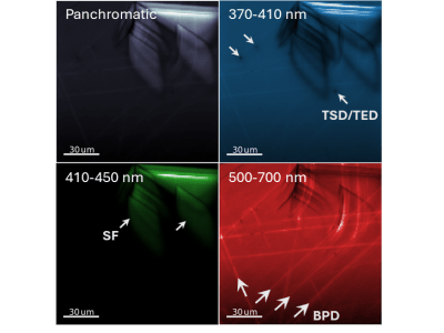
Comprehensive Defect Review and Classification for SiC
We show how spectrally-resolved quantitative CL can be used to classify various defects in SiC
Text Link
Application

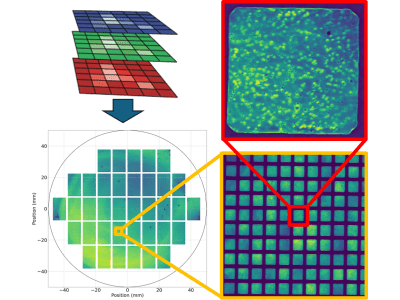
Non-Destructive Quality Control of Micron-Sized Light Emitting Diodes
We introduce CL as a non-destructive method for micro LED process control and development
Text Link
Application

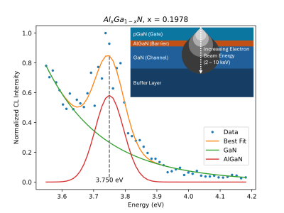
Non-Destructive Control of Epitaxial Layer Uniformity in GaN Power Devices

We show how spectrally-resolved quantitative CL can be used to monitor buried alloy layer composition

Scientific references

Sodium induced beneficial effects in wide bandgap Cu (In, Ga) S2 solar cell with 15.7% efficiency VALLUVAR OLI, Arivazhagan, KAUR, Kulwinder, MELCHIORRE, Michele, et al. Progress in Photovoltaics: Research and Applications, vol. 34, no 4, p. 439-452. 2026
Link between graphene features and the resulting functionality of quasi-van der Waals Zn3P2 HAGGER, Thomas, RABELO FREITAS, Helena, MASTROPASQUA, Chiara, et al. CrystEngComm, vol. 28, no 3, p. 635-648. 2026
High-Resolution Cathodoluminescence Mapping for Doping Quantification across a Wide Range of Silicon Concentrations in GaN Epitaxial Layers M’QADDEM, Zakariae, ROCHAT, Névine, JACOPIN, Gwénolé, et al. Nano Letters, vol. 26, no 16, p. 5514-5521. 2026
Synthetic gain for electron-beam spectroscopy CHEN, Yongliang, ZENG, Kebo, XIE, Zetao, et al. Nature Communications 2026

Scientific references

Cathodoluminescence, light injection and EELS in STEM: from comparative to coincidence experiments TIZEI, Luiz HG, AUAD, Yves, CASTIONI, Florian, et al. Microscopy, vol. 75, no 2, p. 129-144. 2026
Nanoscale Optical Inhomogeneities From Compositional Segregation Within Individual GaN‐on‐Si Quantum Wells Chung, J. Y., Mishra, T. P., Mahfoud, Z., Gage, T. E., Wen, J., Rice, K. P., ... & Bosman, M. Advanced Science, e76414. 2026
Operando Multimodal Electron Microscopy of Perovskite Nano-LEDs: Nanoscale Degradation and Recovery Behavior Nguyen, L. L., Tizei, L. H., Fiedler, S., Auad, Y., Andersen, I. M., Boothroyd, C., ... & Lam, Y. M. ACS nano 2026
Improved interface passivation in high-efficiency Se-alloyed CdTe solar cells using a SnO2/ZnO n-type bilayer LIU, Xiaolei, KUJOVIC, Luksa, ZHOU, Zhaoxia, et al. Solar Energy Materials and Solar Cells, 2026, vol. 297, p. 114139. 2026

Ready to revolutionize your materials characterization approach?

Get in touch with us today to discover how our state-of-the-art cathodoluminescence tools can elevate your research and industry applications.
Already more than 30 systems installed globally!