Light Collection / Injection for STEM
The Mönch is an advanced add-on for coupling light into and out of STEM microscopes, perfect for cathodoluminescence spectroscopy and a wide range of light injection applications.

About Our STEM-CL + Light Injection Solution
Whether operating in light collection or light injection mode, the Attolight Mönch offers a unique feature set that ensures excellent optical performance and user experience.
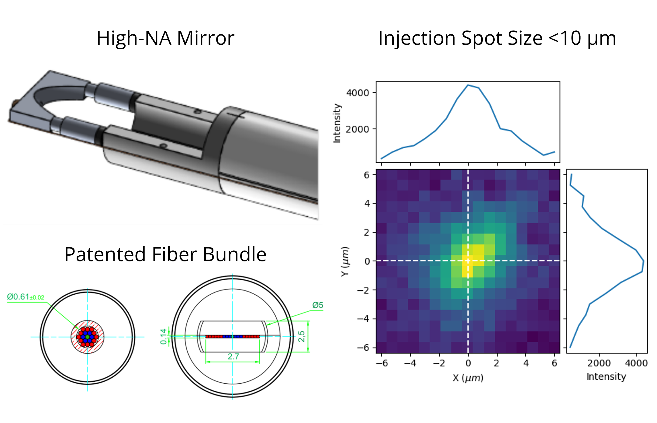
The specially designed, high-NA mirror has been optimized for maximum light collection efficiency and minimum ultimate injected spot size. The precise and reproducible motion control system means less time spent aligning, more time spent collecting data and running experiments. And because the mirror moves independently from the sample holder, you can explore the full surface of your TEM grid while maintaining alignment at eucentric height.
The Mönch is simple to operate and compatible with a wide range of microscopes and complementary techniques, like EELS and EDX.
From CL to pump-probe to in-situ and beyond, the Mönch unlocks a world of possibilities for advanced studies in (S)TEM.
Unique Features for Every Mode of Use
Collection Mode (CL)
In collection mode, the Mönch features several important advantages over other STEM-CL solutions:
- Quick and easy optical alignment for every sample, performed in-situ
- No limitation on which regions of your sample are accessible for CL
- A patented optical fiber which preserves brightness and spectral resolution
Light Injection Mode
In injection mode, the Mönch benefits from tight focusing and optical flexibility:
- A <10 micron-sized spot for localized sample excitation
- Free space coupling ensures compatibility with a wide range of lasers
- Feedback about alignment condition using an in-line detector
Switching between modes is quick and easy, allowing users to adapt their workflow on the fly.
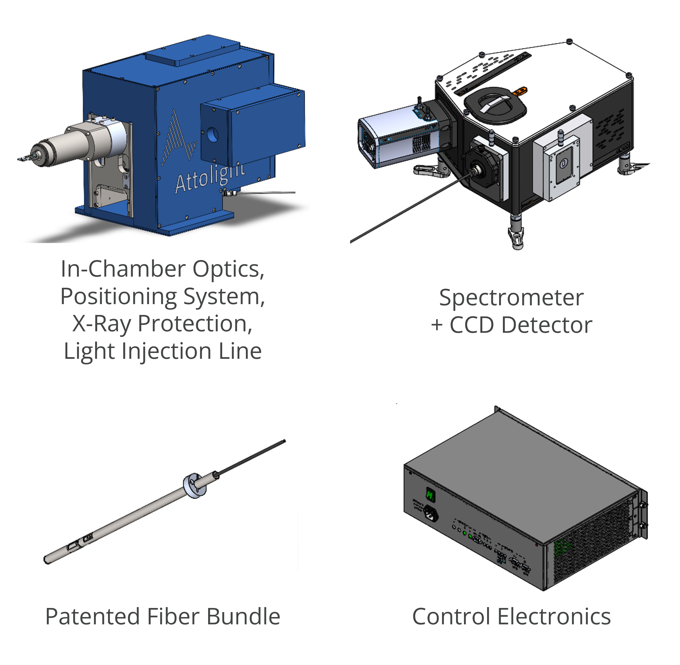
Components of the Mönch
Every component of the Mönch has been meticulously designed for an optimal user experience.
At the heart of the Mönch is a precision engineered mirror which has been optimized for light collection and injection. This mirror is affixed to a sub-micron mechanical positioning system which incorporates additional optics to facilitate getting light into and out of the chamber. In Light Collection Mode, the patented optical fiber bundle is inserted close to the mirror, bringing light to a detection unit, consisting of a high-performance spectrometer and CCD detector. Motion, acquisition, and safety features are controlled by custom electronics for a smooth and seamless user interface.
The default Injection + Collection system is versatile and supports a broad range of wavelengths and applications.
For specialized use cases and customization options, contact us for more information on what might be possible.
Sample Holder Compatibility
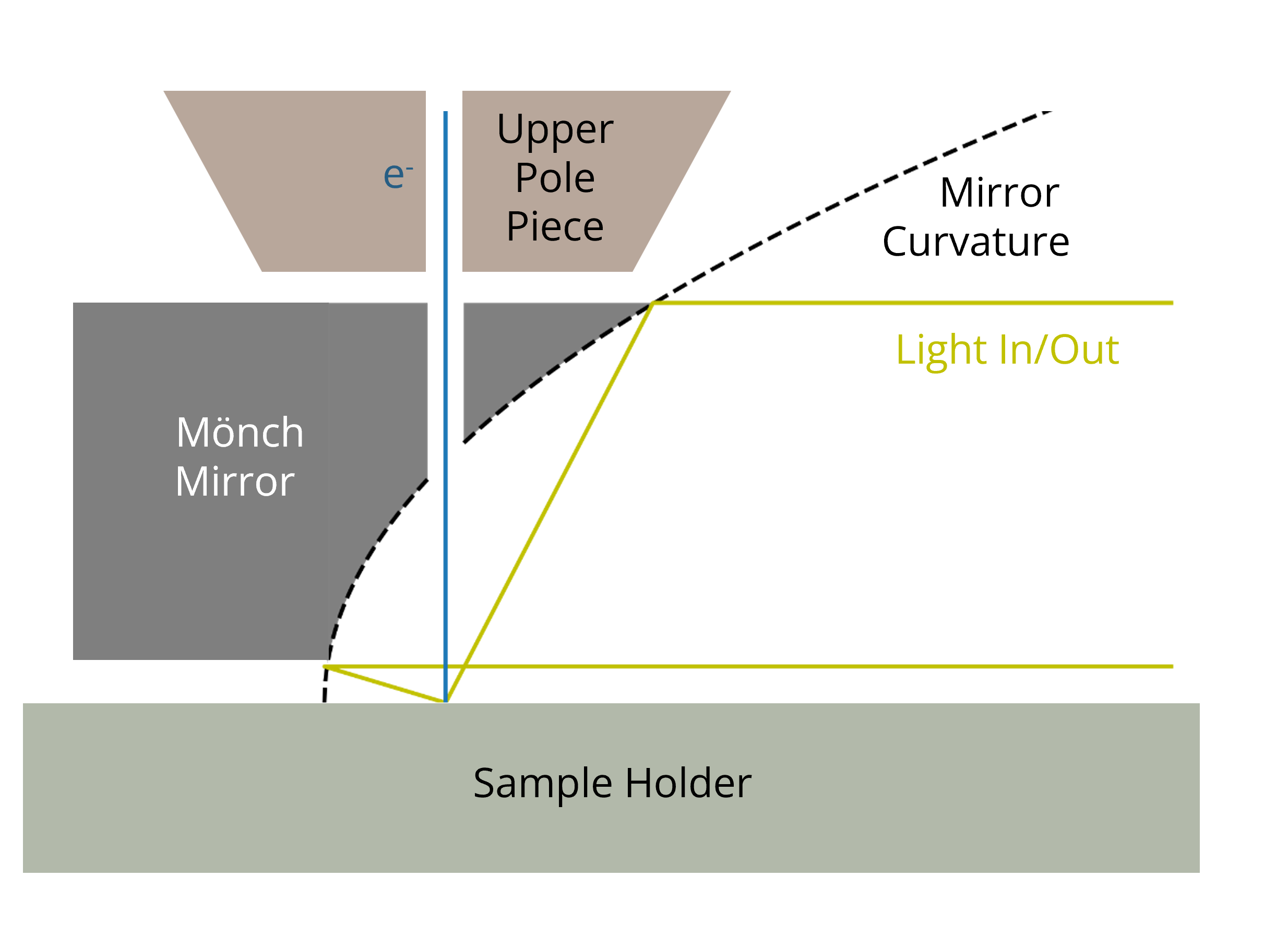
Due to the small space inside the TEM chamber and the unique geometry of the Mönch mirror, only certain sample holders may be used with the Attolight Mönch. Specifically, holders must be thin on their top side and very flat. Tilting is not possible when using the Mönch.
Despite these constraints, there is already a wide range of Mönch-compatible sample holders for various types of experiments, including standard room-temperature, liquid nitrogen cryo, helium cryo and liquid cell holders.
Attolight is proud to work closely with holder companies to ensure compatibility and user convenience, and we’re committed to expanding the range of holder offerings to our customers.
For questions on available holder types and ongoing developments, please contact us or the TEM manufacturer.
Trusted by top semiconductor companies and prestigious research institutes worldwide


Related Applications Using the Mönch Add-On
Discover how an Attolight system can support your research.
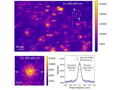
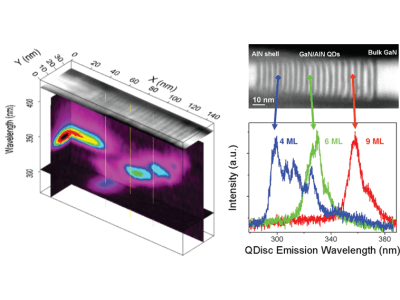
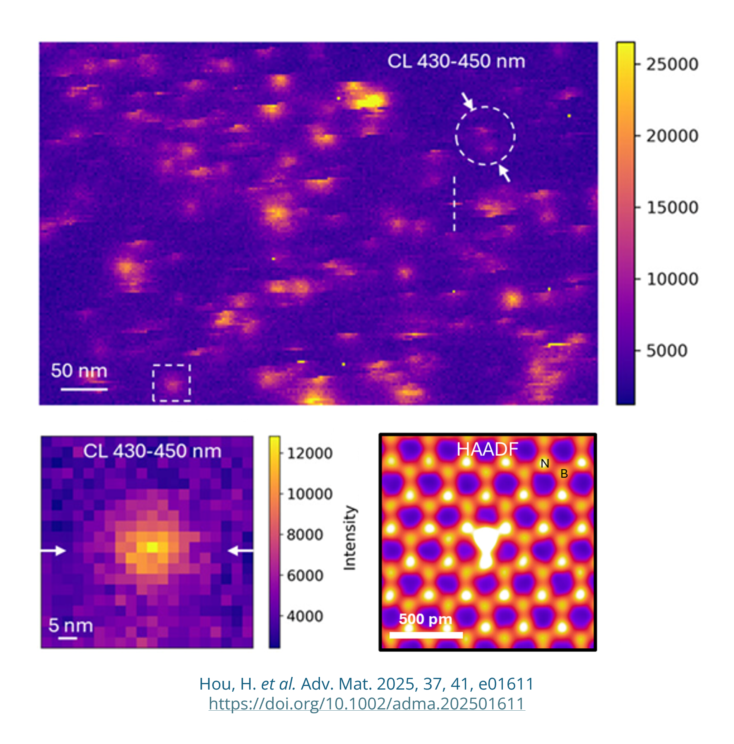
Identifying Atomic-Scale Defects Responsible for Blue Emission in hBN Using Correlative STEM-CL
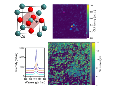
Correlating Structural and Optical Properties of Lead Halide Perovskites