Dislocation Type Determination by Cathodoluminescence

Threading dislocations (TDs) in GaN epitaxial layers negatively impact the performance of semiconductor devices, with different TD types (edge, screw, mixed) having varying effects. While conventional cathodoluminescence (CL) imaging can reveal TD density, it struggles to distinguish between TD types. This study introduces a non-destructive method that uses CL hyperspectral imaging to differentiate TDs, particularly screw TDs. This approach expands dislocation analysis, supporting the optimization of GaN-based devices.
Threading dislocations (TDs) are extended defects that form during the growth of epitaxial layers, such as the ones that serve as the basis for the fabrication of GaN HEMT devices. These defects run roughly parallel to the growth direction and are suspected to negatively impact the yield, performance, and lifetime of final devices.
Depending on their Burgers vector (Bv) ( b ), TDs can be further categorized into edge ( b =na), screw ( b =mc), and mixed (( b =na+mc)) types, where a and c are the GaN lattice vectors. It is well accepted that the negative effects of TDs on devices are strongly dependent on their Burgers vector [1]. In particular, pure screw TDs are suspected to act as current leakage paths.
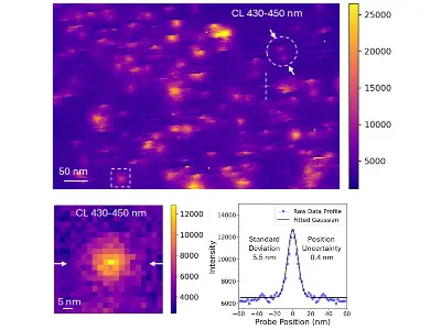
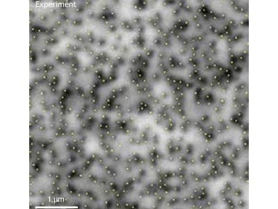
Due to an increased non-radiative recombination (NRR) rate near their core, TDs appear as dark spots in cathodoluminescence (CL) intensity images (Figure 1).

Such images are commonly used to measure TD density. An accurate result can be obtained for TD densities exceeding 109 cm-2. Although the darkness level of the spots may in some cases provide information on the TD type [1, 2, 3], it is not sufficient to differentiate pure screw TDs from other types.
TDs also induce a strain field around them, which varies with the TD type. Strain fields have an influence on the CL signal. Careful analysis of CL spectral and intensity variations around TDs allows to determine their type. In Figure 2a and b, 1c is a single screw TD. 1a is a single edge or mixed TD. Pa and Pb are two types of TD pairs. Variations in CL intensity and peak center energy around TDs are also visible in the cross-sections shown in Figure 2c and d.
In conclusion, by combining CL intensity and peak center energy images, pure screw TDs can be differentiated from other types in a single, non-destructive step.

This study has been co-financed by the All2GaNEuropean project: https://all2gan.eu/home


[1] Y. Yao et al., “Correlation between structural properties and nonradiative recombination behaviors of threading dislocations in freestanding GaN substrates grown by hydride vapor phase epitaxy,” CrystEngComm, vol. 22, no. 48, pp. 8299–8312, 2020, doi: 10.1039/D0CE01344G.
[2] T. Hino, S. Tomiya, T. Miyajima, K. Yanashima, S. Hashimoto, and M. Ikeda, “Characterization of threading dislocations in GaN epitaxial layers,” Appl Phys Lett, vol. 76, no. 23, pp. 3421–3423, Jun. 2000, doi: 10.1063/1.126666.
[3] M. Albrecht, J. L. Weyher, B. Lucznik, I. Grzegory, and S. Porowski, “Nonradiative recombination at threading dislocations in n-type GaN: Studied by cathodoluminescence and defect selective etching,” Appl Phys Lett, vol. 92, no. 23, p. 231909, Jun. 2008, doi: 10.1063/1.2928226.
Source:
“GaN Epitaxial Defects Characterization Using Cathodoluminescence Spectroscopy”, M. Fouchier, C. Monachon, M. Davies, ISTFA proceedings 2023, pp. 463-468.


.webp)

