Non-Destructive Quality Control of Micron-Sized Light Emitting Diodes
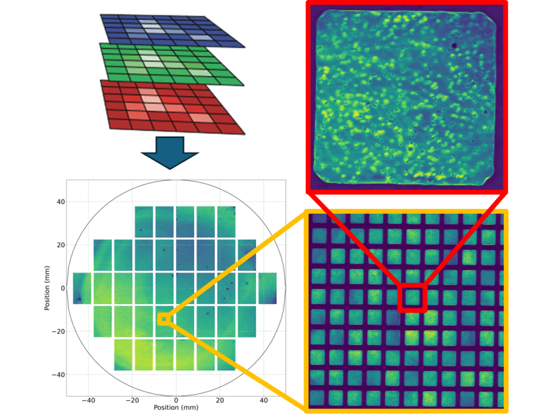
MicroLEDs, or microstructured inorganic LEDs with sizes significantly below 100 µm, currently pose a unique challenge in terms of metrology and process development. Indeed, feature size is increasingly challenging to resolve for regular photoluminescence-based techniques, and high-resolution imaging is required for checking device homogeneity. Cathodoluminescence spectroscopy offers a combination of high-resolution and photo-spectroscopic capabilities that make it uniquely appropriate to tackle this challenge.
High-performance microLED products currently rely on end-of-line electroluminescence (EL) probing for final testing and binning. In-line characterization is also possible using photoluminescence (PL) or automated optical inspection (AOI), though these techniques have reduced spatial resolutions and cannot predict certain kinds of failure.
Cathodoluminescence (CL) offers a scalable approach to in-line microLED metrology that can reduce the turnaround time between inspection and process intervention, lowering the amount of product at risk. CL can also offer deeper insights for both process control and process development. With both imaging and spectroscopy acquisition modes, CL is an adaptable technique that is well-suited to both industry and R&D environments.
As an example, panchromatic maps (integrating the intensity over all wavelengths) or monochromatic maps (measuring the intensity of one particular wavelength) can be made quickly over large fields of view. By scanning over the surface of a wafer, a full-wafer map can be generated, providing valuable information on emission uniformity, defectivity, and the origin of process variations.
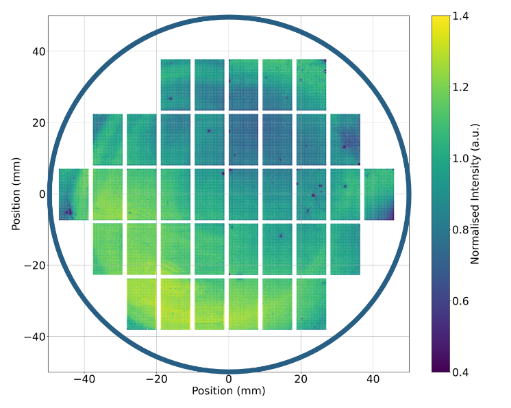
Figure 1 demonstrates the utility of CL screening for process control applications. The panchromatic wafer map reveals dark spots which correspond to luminescence-killing defects, as well as significant variation in the intensity of light emitted from different regions of the wafer. The underlying pattern of this variation can be correlated to certain process steps, such as the epitaxy itself or subsequent removal processes, to identify and contain process excursions from problematic tools or chambers.
Moving from the macro to the micro or even nano scale, SEM and panchromatic or monochromatic CL maps can be acquired in parallel for further in-depth review. This data helps identify and correlate defects to changes in luminescence, combining the benefits of AOI and PL in one, with the advantage of better spatial resolution.
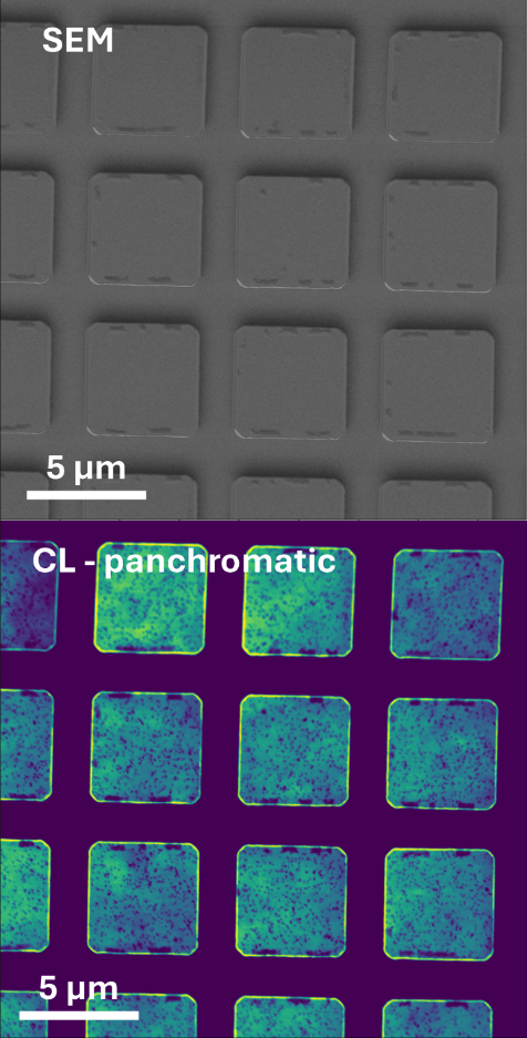
In Figure 2, the array of microLEDs appears mostly regular and uniform when viewed by SEM, with a few minor cosmetic defects and morphological inhomogeneities. In the corresponding panchromatic CL image, however, we observe sub-micron dark regions where luminescence is significantly reduced, as well as important variations in overall luminescence intensity from one microLED to the next. Attolight’s collection optics ensure that these intensity variations can be reliably quantified and attributed to the sample investigated, rather than to the analysis tool itself.
Interestingly, some, but not all, of the dark spots correspond to visible defects, implying that there are other defects under the surface that cannot be seen by SEM or AOI. Conversely, some, but not all, of the cosmetic defects seen by SEM translate into dark regions in the CL map, implying that, from a process and quality control perspective, some cosmetic defects can be tolerated.
Targeted investigations using panchromatic CL maps are ideal for understanding the impact of both visible and invisible defects on microLED performance. Thanks to the large field of view of Attolight’s CL microscopes and their quick and easy alignment procedure, rapid but detailed panchromatic or monochromatic CL screening can also be used as part of a process control metrology strategy using either random or systematic sampling.
In addition to panchromatic screening, hyperspectral CL imaging, where one records a unique spectrum at every pixel in an image, opens the door for even more advanced analysis into the origin and impact of process variations. Such acquisitions can be particularly useful for process development applications.
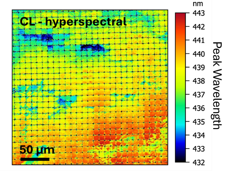
In Figure 3 we plot the change in the emission peak wavelength over a 225 µm field of view for an array of InGaN microLEDs. We see that the peak emission wavelength varies over a range of more than 10 nm, and this shift can be spatially correlated to different regions within the field of view; some areas exhibit redshift while other areas exhibit blue shift. By using CL hyperspectral imaging, such undesirable inhomogeneities can be quickly and easily identified for root cause analysis, resulting in improved product quality. The Attolight CL’s scalable spatial resolution means that hyperspectral maps can be used to study individual pixels or large ensembles within the array.
With its advanced, integrated optics that allow for fast and reliable optical alignment and consistent, quantitative results, the Attolight CL system opens new possibilities for both in-line process control and R&D applications. Hyperspectral maps are rich in information, giving insight into the source and impact of process variations and defects, both underlying and cosmetic, at resolutions unmatched by competing techniques like PL. With fast panchromatic and monochromatic imaging, large surfaces of production wafers can be screened long before end-of-line inspection, shortening the feedback loop for process control operations. In both ways, Attolight’s CL solutions help to bridge the gap left by current metrology and analysis techniques.



.webp)
