
Angstrom Scientific as new US representative
Angstrom Scientific Inc. will distribute Attolight q-CL equipment in North America
Lausanne-Switzerland – Dec 12, 2022 – Attolight AG announces the appointment of Angstrom Scientific Inc., as the North American (USA, Canada) distributor of its quantitative Cathodoluminescence (q-CL) equipment range. It features its automated solution for semiconductor inline defect inspection (Säntis 300) and its high-end material research tools in industrial R&D and academia (Allalin, Mönch). q-CL is a quantitative and non-destructive characterization method that produces spectroscopic data at the nanoscale and provides a deeper understanding of the structure of materials.
To better reach potential users of this technology, Attolight AG has entered into a distribution agreement with Angstrom Scientific Inc., a leading source for microscopy and spectroscopy products. Samuel Sonderegger, CEO of Attolight AG, was excited at the possibilities this new partnership would provide, “Angstrom Scientific is very well known in the field of electron microscopy and nano-science. Their relationships and history with researchers and institutions in this market will provide new opportunities for q-CL products to reach the people who will benefit most from their adoptions in the lab.”
Bob Sommerville, CEO of Angstrom Scientific Inc., commented, “We are delighted to have the opportunity to work with the Attolight team, and to have the Mönch, Allalin and Säntis 300 spectroscopic CL products in the Angstrom portfolio. As we have gotten to know the management team we have the utmost confidence that we can continue to advance the Attolight presence in the North American market. The requirement to have high resolution defect inspection is only going to continue to grow and Attolight are in an excellent position to address this growing market”
For further information on how Attolight CL can be utilized to support your research, please contact either Angstrom Scientific Inc. (https://www.angstrom.us/) or Attolight (https://www.attolight.com/).

Ultimate GaN project
After 3.5 years of project work, the Ultimate GaN Project dedicated to research for GaN technologies, devices and applications and aiming at addressing the challenges of the future GaN roadmap ends with major breakthroughs. Attolight has been pleased to be a part of these developments.
EU research: Energy-saving chips made of gallium nitride boost efficiency and CO2 savings
European research team developed compact, low-cost energy-saving chips made of the semiconductor material gallium nitride. This opens up a new dimension of energy efficiency in wireless charging of electric cars, in integrating renewable energies into the power grid and enables a sustainable 5G rollout.
The urgent energy transition, the reduction of CO 2 emissions and the rising demand for energy are challenging topics of our time. Efficiency is more important than ever before. Generating, controlling and using energy efficiently is a crucial lever for digitalization and decarbonization. Smart technologies and new semiconductor materials such as gallium nitride (GaN) play a key role here. GaN power semiconductors deliver more power in a small space, save energy and thus minimize the CO 2 footprint.
New energy-saving chips
In the "UltimateGaN" research project, a team from science and industry has set itself the task of making the advantages of GaN technology usable for many applications. The results are groundbreaking. Further developments in materials and process technology have made it possible to provide efficient and compact GaN energy-saving chips at globally competitive costs in the future. Many applications can benefit from this - from wireless charging of electric cars to the low-loss, smooth connection of solar energy to the grid and the rapid, cost-effective expansion of 5G networks.
Wireless charging of e-cars
In terms of energy efficiency, for example, the prototype developed for wireless charging of e-cars was able to transmit energy with an efficiency level of 96 percent. By comparison, systems available on the market currently deliver efficiencies of 93 percent at most. A three-percent improvement in energy efficiency offers the potential to achieve a reduction of around 1.7 megatons of CO 2 per year by 2030, which is roughly the same amount as emitted by around one million cars with internal combustion engines.
Sabine Herlitschka, CEO of Infineon Technologies Austria AG: "Energy efficiency is one of the world's greatest resources for saving energy and reducing CO 2 emissions. Power semiconductors made of gallium nitride are real pacesetters for sustainability. The results show how research from Europe is making a decisive contribution to energy efficiency. Every percentage point counts and is a contribution to the European Green Deal. As a global competence center for new semiconductor materials such as gallium nitride, Infineon coordinated this project and achieved decisive further developments together with its partners. This is the best basis for sustainable innovations 'developed and made in Europe'. "
"UltimateGaN is a flagship research project because it combines the competencies of 26 partners from 9 EU countries and enables improvements in the entire GaN value chain: from research work on the material to process development, design, packaging and system solutions," explains Herbert Pairitsch, Director Technology & Innovation at Infineon Technologies Austria and overall project manager, adding, "The results from research, development and manufacturing are linked and the entire process becomes more efficient and climate-friendly. This will benefit the partners directly and subsequently many other industries."
GaN revolutionizes energy use
In semiconductor technology, the raw material GaN, which is a by-product of aluminum production, can unleash its full physical potential. GaN semiconductors are more heat-resistant, produce more power, convert energy much faster and thus have fewer energy losses. The energy savings mean that GaN also benefits the environment, as there are fewer emissions. The benefits are already being seen in LED lights and in power supplies in consumer electronics. Compared with other charging solutions, GaN reduces energy losses here by 21 percent. Research in the "UltimateGaN" project is now making high-performance GaN chips usable for other applications.
Research brings more efficiency in design and process
In the "UltimateGaN" project, high-performance GaN layers were realized on 200-millimeter silicon wafers and tested in various applications. In combination with advanced metallization processes, optimized assembly and interconnection technologies as well as design adaptations, it was possible to improve the overall GaN system structure of the GaN microchip and to further reduce the size. The technological advantages of GaN are combined with process improvements in the manufacturing process.
In a nutshell this means that smaller designs bring smaller housings, less material and resource consumption, better productivity in manufacturing and thus lower production costs. In the end, many applications worldwide benefit from this in order to save energy and minimize the CO 2 footprint. Three applications were specifically addressed in the project: smart mobility, smart grid and 5G communication networks.
Smart Mobility: Wireless charging of e-cars
GaN components are particularly useful in efficiency-driven applications such as charging electric cars. If this is also done wirelessly, the ease of use also increases at the same time. The research team developed a bidirectional 3.6-kW battery charger with GaN power converters for this purpose. The prototype achieved an efficiency level of up to 96 percent, clearly surpassing previous efficiencies of 90 to 93 percent. The underlying inductive charging technology also works in snow and ice and is also practical, for example, in places where vehicles are often found, such as supermarket parking or city parking lots.
Smart grid: integration of renewable energies
There is also great potential in energies from the sun and wind and their integration into the power grid. Intelligent power electronics minimize energy conversion losses and get more electricity out, so to speak. To this end, the project implemented a modular GaN conversion concept for the integration of microgrids - i.e. local subgrids consisting of photovoltaics, wind and storage technologies - into the smart grid. More than 3,000 hours of field tests prove that the GaN components offer the best reliability with the highest efficiencies of up to 98.4 percent and thus decisively advance the energy transition.
5G communication: Fast data transfer
Research also lays the foundation for GaN amplifier modules and thus for fast data transfer, for example, for lightning-fast video streaming or communication in the Internet of Things. Since the energy-efficient 5G amplifiers made of GaN are also more cost-effective, a faster, more energy-efficient and climate-friendly 5G-rollout will be possible. The project also won the 2019 Futurezone Award in the 5G category.
The results of "UltimateGaN" show great potential and are of significant societal benefit - for a digital and sustainable future.
EU cutting-edge research: 26 partners from nine countries
The European project "UltimateGaN" (Research for GaN technologies, devices and applications to address the challenges of the future GaN roadmap) ran for a total of three and a half years. The project volume of 48 million euros was financed by investments from industry, grants from the individual participating countries and the ECSEL Joint Undertaking (Electronic Components and Systems for European Leadership).
The project partners are:
Austria: Austria Technologie & Systemtechnik AG, Infineon Technologies Austria AG, Fronius International GmbH, SAL Silicon Austria Labs, Graz University of Technology | Belgium: IMEC | Germany: AIXTRON SE, Infineon Technologies AG, Siltronic AG, Max Planck Institute for Iron Research GmbH, Fraunhofer Gesellschaft zur Förderung der angewandten Forschung e.V., Chemnitz University of Technology, NaMLab GmbH | Italy: Università degli studi di Padova, Infineon Technologies Italia, Universita di Milano Bicocca | Norway: Eltek AS | Slovakia: Slovak University of Technology in Bratislava, Nano Design SRO | Switzerland: Ecole Polytechnique Fédérale de Lausanne EPFL, Attolight SA | Spain: IKERLAN, For Optimal Renewable Energy, LEAR | Sweden: RISE Research Institutes of Sweden AB, SweGaN AB
More links:
- Project website: www.ultimategan.eu
- Project results brochure: UltimateGaN - Enabler for green applications
- Project video: Video with results
ER-C’s Electron Microscope Receives Unique Upgrades
Forschungszentrum Jülich operates some of the most powerful electron microscopes in Europe at the Ernst Ruska-Centre for Microscopy and Spectroscopy with Electrons (ER-C), in part together with RWTH Aachen University. The instruments not only make it possible to study the structure and composition of materials with sub-Ångstrom spatial resolution, but also to determine their local functional properties.
Such capabilities are essential for the development of innovative new materials, such as those needed for information and energy technology. In cooperation with partners from science and industry, including the Swiss company Attolight AG, a project is now underway to install ground-breaking upgrades to one of the electron microscopes in the ER-C. These upgrades are intended to allow nanoscale magnetic structures and their dynamics to be analyzed under light illumination with unprecedented spatial resolution. The project is funded through the ERC Synergy Grant “3D MAGIC” of the European Research Council. The aim of 3D MAGIC is to study still largely unknown nanoscale magnetic structures that have particle-like properties and whose existence has so far only been predicted theoretically.
A prototype ultra-high-resolution aberration corrected electron microscope was developed in the 1990s in collaboration with Jülich, and is still on site at the ER-C today. Since then, the need for ever more sophisticated analysis has driven further technical and methodological developments in Jülich, often in cooperation with industry. Another important stage is now beginning: Forschungszentrum Jülich has signed a contract with the company Attolight AG to order customized components for a unique upgrade of its Titan “Holo” microscope.
From 2022, this upgrade will enable the study of light-matter interactions with unprecedented spatial resolution. A strong focus of the project involves the study of 3D magnetic solitons, which are extremely puzzling and challenging research objects that range from a few nanometres to a few hundred nanometres in size, only occur in certain magnetic materials and offer prospects for new types of information storage for so-called neuromorphic computing - energy-efficient computing modelled on the human brain.

- Researchers are looking to study magnetic nanostructures that are termed “hopfions”.
Copyright: Forschungszentrum Jülich
At the ER-C, off-axis electron holography is being used to measure the magnetic fields of nanostructures with high spatial resolution. The technique is based on the interference of two electron beams and allows the recovery of the electron optical phase shift of the electrons. The technique provides direct and quantitative information about magnetic fields in materials on the nanometre scale. The new instrumentation aims to make it possible to apply external magnetic fields, temperature gradients and electrical currents, in combination with laser illumination, to a sample inside the electron microscope.
At the core of the upgrade is a light injection system (Mönch) manufactured by Attolight. This add-on enables light to be injected into the electron microscope by focusing a laser beam onto a specimen with a very small spot size (below 2 µm in diameter). The system offers both light injection and collection for wavelengths ranging from the ultraviolet to the infrared. In this project, the light source will be used to carry out dynamic measurements of the magnetic properties of materials in the sub-µm range.
The concept for the upgrade was developed at Forschungszentrum Jülich. Several other institutes in Jülich are involved in the project, including PGI-1, PGI-6 and the Central Institute of Engineering, Electronics and Analytics (ZEA), as well as companies that will supply lasers, special magnetic coils, sample holders and software for automation of experimental workflows. Scientists in the ER-C are among a small number of experts worldwide able to image magnetic structures that are just a few nanometres in size. Attolight is extremely proud to participate in the upgrade of the Titan Holo microscope in Jülich and to contribute to the achievement of new breakthroughs in the field of magnetic imaging.

The Titan Holo microscope at Forschungszentrum Jülich stands taller than an average person. From 2022 onwards, after the planned upgrades, it will be possible to apply local magnetic fields, electrical currents and optical stimuli in this microscope to study the magnetic properties of nanoscale materials at cryogenic temperatures.
Copyright: Forschungszentrum Jülich
Further information:
Press release from Forschungszentrum Jülich “ERC Synergy Grant: 12 Million Euros for research into “magic” 3D nanostructures” from 11.10.2019

International Conference on Display Technology
Attolight as invited speaker at ICDT 2021
Attolight will attend the 2021 Edition of ICDT (International Conference on Display Technology) from May 30 to June 2, 2021. This ). ICDT is the only display technology conference held solely by SID outside the United States. The event gathers top scientists, engineers, corporate researchers, and business people of the display industry.
Our Head of Industry Applications, Matthew Davies will give a talk during the session ‘Micro LED Applications.
We welcome you to attend his presentation on ‘An Alternative Method for Cost Effective Probing in MicroLEDs’ on Wednesday, June 2/15:40 (Session 53.1).
For more information on the conference: https://www.sidicdt.org/en/
Full program of the conference: https://www.sidicdt.org/en/col.jsp?id=165

SEMICON Europa 2021
Fell free to visit our German representative Merconics (booth B1650) during the Semicon Europa 2021 (Munchen-Germany, Nov 16-19, 2021).
Conference website: https://www.semiconeuropa.org/
Agenda : https://www.semiconeuropa.org/programs-catalog/agenda-at-a-glance
CS International Conference 2021
Attolight presentation on Cost-Effective Probing in High Volume Manufacturing of MicroLEDs
Attolight will attend the 2021 Edition of CS International from November 9th - November 10th 2021.
Our CEO, Samuel Sonderegger will give a talk during the session Seeking new opportunities for LEDs and lasers on Tuesday, November 9th.
Drop by our booth to learn more about our cathodoluminescence R&D and metrology solutions.
For more information on the conference: https://csinternational.net/
Full program of the conference: https://csinternational.net/agenda
Meet us at CS International 2022 (June 28-29, Brussels)
Attolight presentation on Cost-Effective Probing in High Volume Manufacturing of MicroLEDs
Attolight is pleased to invite you to the 2022 Edition of CS International on June 28-29, 2022 (Brussels, Belgium) and the talk (June 29th, 14:05) on Cost-Effective Probing in High Volume Manufacturing of MicroLEDs given by Samuel Sonderegger.
For more information on the conference: https://csinternational.net/
Full program of the conference: https://csinternational.net/agenda
Attolight as invited speaker at Display Week 2021
Attolight will attend the 2021 Virtual Edition of Display Week (May 17-21, 2021) that will gather the international specialists of OLED, MicroLED, AR/VR/MR, printed displays. This event includes the most influential companies in the business of display. In this frame, our Head of Industry Applications, Matthew Davies, is invited to give a talk during the session ‘Micro LED Display Metrology’.
We welcome you to attend his presentation on ‘Cost Effective Probing in High Volume Manufacture of µLEDs’ on Thursday, May 20th afternoon (Session 58.2).
For more information on the conference: http://www.displayweek.org/
Full program of the conference: http://www.displayweek.org/Portals/5/pdf/2021%20Preliminary%20Program.pdf
Abstract
Cost Effective Probing in High Volume Manufacture of µLEDs
Matthew Davies, Attolight AG-Switzerland
Cost-effective probing of µLEDs in mass-production presents a new series of challenges associated with the greatly increased quantity and density of devices per wafer, specifically regarding measurement time, spatial resolution, and wafer throughput. Here we present a cost appropriate probing solution for wafer level metrology of µLEDs, specifically designed to address the need for post-frontend device verification.
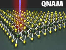
A Novel Technique to Probe Optical Absorption of 2D Materials by Cathodoluminescence
Nano Letters has recently reported a novel technique to map the optical absorption of two-dimensional materials. It is a non-contact and non-destructive technique named Quantitative Nanoscale Absorption Mapping (QNAM). The inventors of QNAM come from EPFL (Lausanne, Switzerland), IMEM (Parma, Italy), the U.S. Army (New Jersey, USA) and the Instituto Nanoscienze (Pisa, Italy).
How does it work?
The original approach of QNAM is to probe the absorption properties of a 2D material using the CL emission of the underlying substrate as the light source.
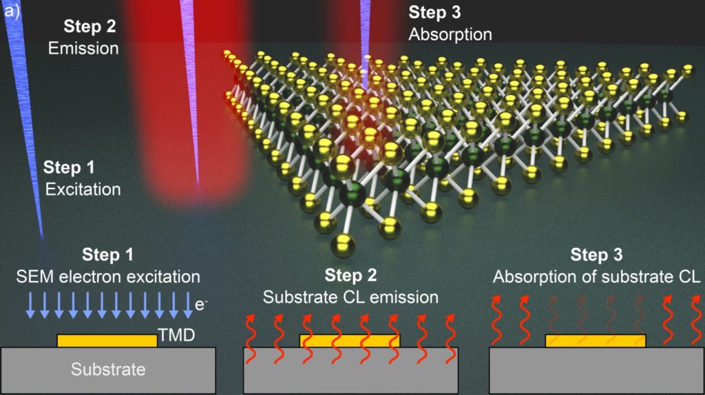
A bulk substrate topped with a two-dimensional layer is excited by an electron beam. As a result, the substrate emits light, via a cathodoluminescence process, that is partially absorbed by the 2D material.
What does it bring?
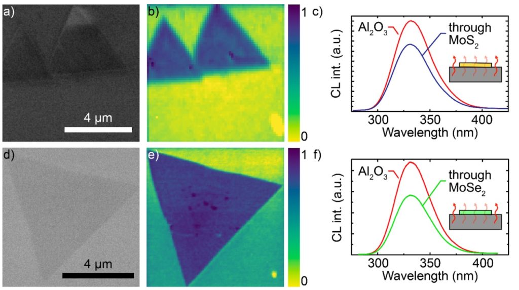
In their report, the authors first noticed an enhancement of the absorption in the UV range due to interlayer excitonic phenomena. Then, they extended the QNAM technique to measure the optical absorption of MoS2/MoSe2 van der Waals heterostructures. Finally, they used it to detect defects such as grain boundaries and ad-layers.
To find out more on the QNAM technique
Quantitative Nanoscale Absorption Mapping: A Novel Technique To Probe Optical Absorption of Two-Dimensional Materials, M.Negri, L.Francaviglia, D.Dumcenco, M.Bosi, D.Kaplan, V.Swaminathan, G.Salviati, A.Kis, F.Fabbri, A.Fontcuberta i Morral, Nano Lett. 2020, 20, 1, 567-576
