Nano Letters has recently reported a novel technique to map the optical absorption of two-dimensional materials. It is a non-contact and non-destructive technique named Quantitative Nanoscale Absorption Mapping (QNAM). The inventors of QNAM come from EPFL (Lausanne, Switzerland), IMEM (Parma, Italy), the U.S. Army (New Jersey, USA) and the Instituto Nanoscienze (Pisa, Italy).
How does it work?
The original approach of QNAM is to probe the absorption properties of a 2D material using the CL emission of the underlying substrate as the light source.
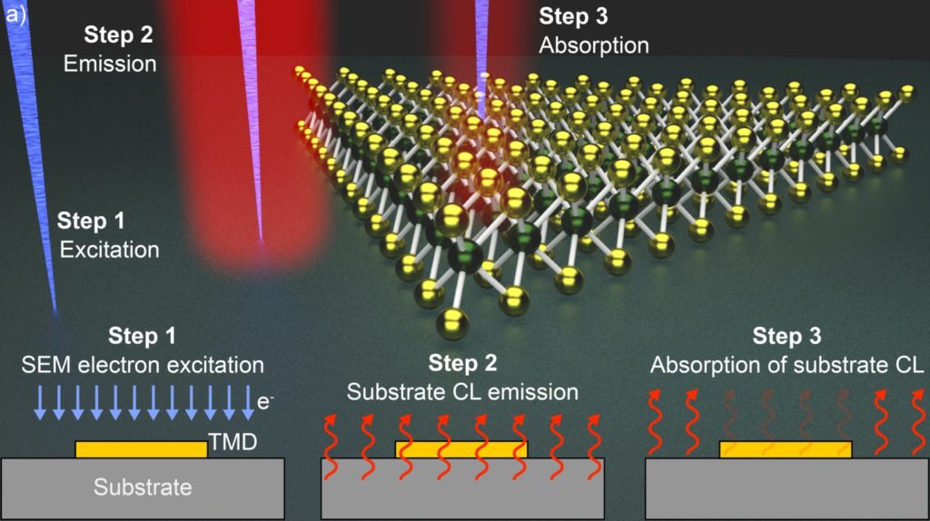
A bulk substrate topped with a two-dimensional layer is excited by an electron beam. As a result, the substrate emits light, via a cathodoluminescence process, that is partially absorbed by the 2D material.
What does it bring?
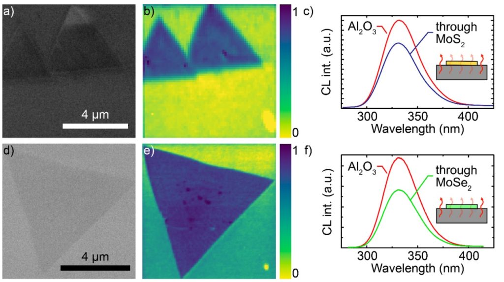
In their report, the authors first noticed an enhancement of the absorption in the UV range due to interlayer excitonic phenomena. Then, they extended the QNAM technique to measure the optical absorption of MoS2/MoSe2 van der Waals heterostructures. Finally, they used it to detect defects such as grain boundaries and ad-layers.
To find out more on the QNAM technique
Quantitative Nanoscale Absorption Mapping: A Novel Technique To Probe Optical Absorption of Two-Dimensional Materials, M.Negri, L.Francaviglia, D.Dumcenco, M.Bosi, D.Kaplan, V.Swaminathan, G.Salviati, A.Kis, F.Fabbri, A.Fontcuberta i Morral, Nano Lett. 2020, 20, 1, 567-576
