
Hyperspectral imaging
Introduction
Hyperspectral imaging is an acquisition mode in which a full spectrum is recorded for every pixel in an image. The result is an information-rich map, called a data cube, that can be used to visualize differences in a sample’s spectral signature across a field of view. The data cube can also be sliced to obtain images within different wavelength bands. Hyperspectral imaging is commonly used in cathodoluminescence (CL) but also in many other spectroscopy techniques.
Principles
CL can involve both imaging and spectroscopy aspects, depending on the application. The most basic approach to CL imaging is known as panchromatic imaging, which produces a 2D greyscale image, where the brightness of each pixel represents the overall CL intensity emitted by the sample across all wavelengths. The most basic approach to CL spectroscopy involves recording individual point spectra, where the electron beam is directed to a single point on the sample and the resulting cathodoluminescence intensity is recorded as a function of wavelength (λ).
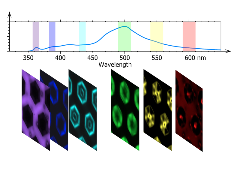
Hyperspectral imaging combines both aspects described above to provide an information-rich data set that can be used for advanced analysis beyond what is possible with standard imaging or spectroscopy alone. To create a hyperspectral image, a full CL spectrum is recorded serially at each pixel of an image in order to build up a 3D hyperspectral data cube. The first two dimensions of the cube are the x and y axes of the image, representing the field of view on the sample. The third dimension is the wavelength axis, representing the CL intensity at each particular wavelength, or “color”, of light. This is illustrated schematically in Figure 1.

Because of the complexity of data contained within a hyperspectral map, there are many ways to visualize it. One could, for example, explore the individual spectra at each pixel, or integrate the spectra over a subset of the image area. One could also create a color image by assigning different wavelength ranges to different colors in a single image (see Figure 3) or create a series of 2D monochrome images (one for each wavelength or wavelength range, see Figure 4).
Hyperspectral imaging can be useful for a variety of applications, including identifying different layers in a film stack, quantifying inhomogeneities in an alloy, classifying defects based on their emission spectrum or even identifying the presence of strain around morphological features.
Instrumentation
The instrumentation required to create a hyperspectral image is simply the standard equipment required for CL spectroscopy: a scanning electron beam (whether SEM or STEM), a light collection system including lenses for collimation and focusing, and a spectrometer equipped with a spectroscopy camera (though a rotating grating and a point detector such as a PMT is also possible). A schematic of a typical setup is shown in Figure 2.
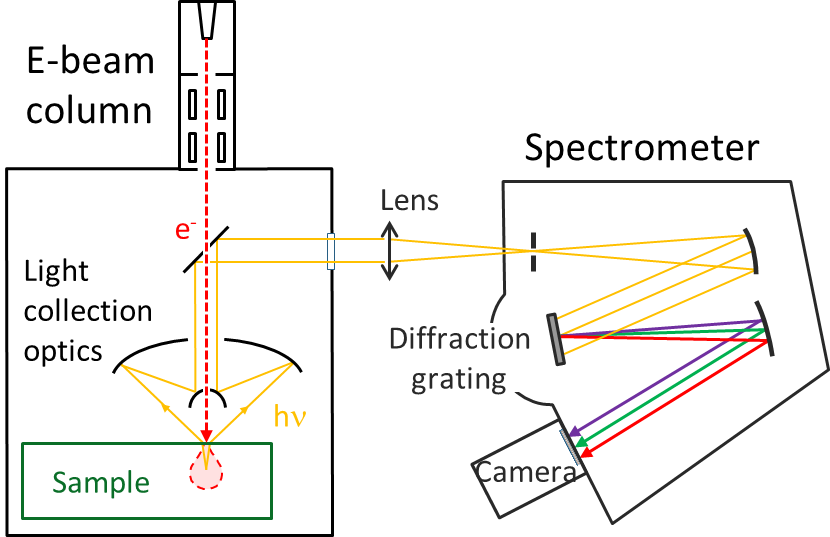
The diffraction grating inside the spectrometer can be selected to provide the optimum efficiency and spectral resolution for the desired wavelength range. Typically, a CCD camera is used to record the intensity at each wavelength simultaneously.
Example results
Example 1
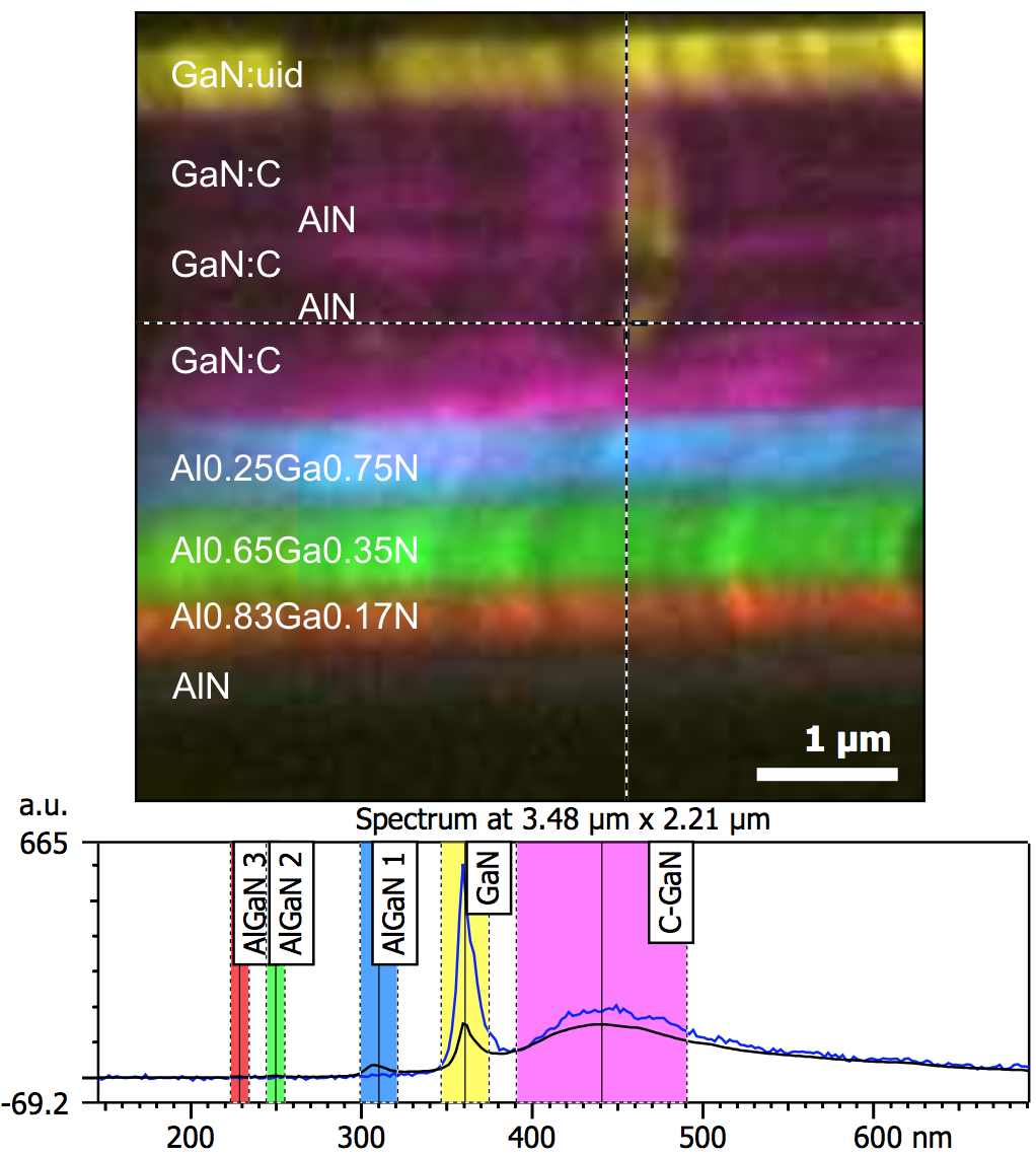
In Figure 3, hyperspectral imaging is used to identify and visualize the different layers in a GaN HEMT film stack as well as to highlight the presence of a punch-through defect. The defect is identified as a streak of unintentionally-doped GaN (GaN:uid, shown in yellow) penetrating the carbon-doped GaN (GaN:C, shown in pink) and AlN layers. Different colors have been assigned to different segments of the spectral range. Intensity of each color is proportional to the number of counts detected in the corresponding range at each pixel.
Example 2
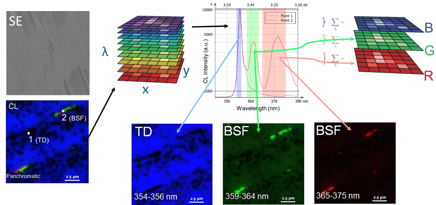
In Figure 4, hyperspectral imaging is used to identify and visualize different defects in a GaN layer. In the CL images, different colors are assigned to different wavelength ranges: the blue band corresponds to near-band-edge (NBE) emission whereas green and red correspond to two different peaks related to basal plane stacking faults (BSFs) in the GaN. Dark spots correspond to threading dislocations (TDs).
Benefits and Further Reading
- Identification of material composition, including gradients and interfaces [2]
- Identification and classification of defects [3]
- Quantifying material inhomogeneity [4]
- Correlation between strain and morphological features
- Failure analysis
- Correlation between microstructure and optoelectronic properties [5]
Latest Scientific Publications
Hyperspectral imaging
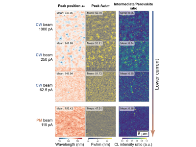
CL from beam-sensitive optoelectronic materials - hybrid halide perovskites
Applications on Semiconducting Diamond
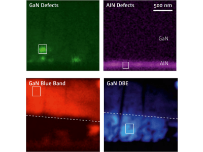
Applications on Hyperspectral Mapping with high Spatial Resolution for Optoelectronic Devices
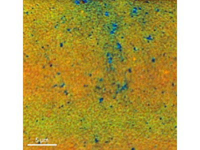
Pinhole Detection in Photovoltaic and Thin Film Battery Materials
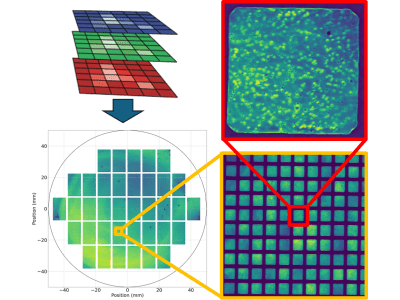
Non-destructive quality control of micron-sized light emitting diodes
Explore our high-resolution cathodoluminescence tools designed for superior materials characterization.


