Cathodoluminescence as a Reliable Method to Quantify Threading Dislocations in InP-Based Optical Devices
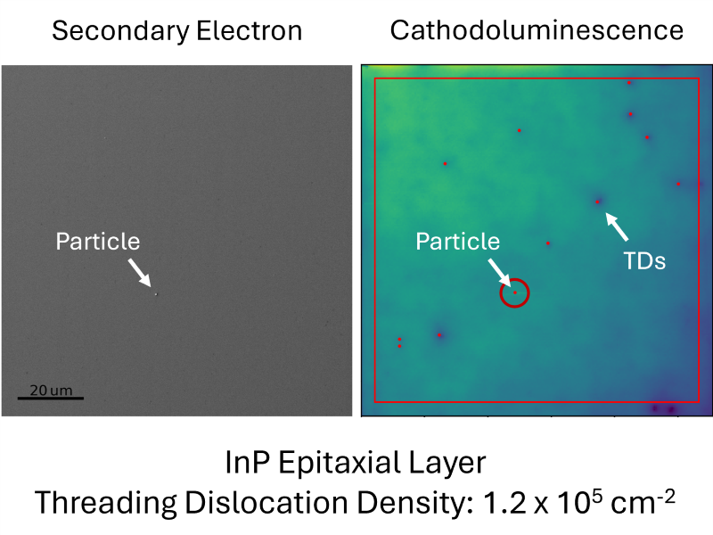
The transition to optical interconnects in data centers relies on InP-based laser diodes coupled to silicon photonic circuits, but device reliability is highly sensitive to threading dislocation (TD) density in the InP epitaxial layers. Conventional metrology techniques—SEM, PL, and XRD—struggle to reliably detect and quantify these defects. This application note demonstrates cathodoluminescence (CL) mapping as the only effective method for identifying and quantifying TDs in InP epilayers. CL reveals TDs as distinct dark spots with high spatial resolution, enabling straightforward defect counting and density estimation (approximately 1.2 × 10⁵TDs/cm² in the sample studied). These results establish CL as an effective, automatable inspection method for monitoring reliability-limiting defects in InP devices—applicable at the substrate, epilayer, and device level—helping manufacturers catch bad devices before they fail in the field.
With the rise of AI, there is growing demand to increase the bandwidth and power efficiency of data transfer between compute units in data centers. This likely means a transition from purely electrical connections toward hybrid electro-optical solutions. InP is the most promising material platform for optical interconnects and high-throughput data communications due to its compatibility with direct bandgap infrared (IR) emission. Generally, this is done using co-packaged optics, in which InP-based laser diodes are integrated onto silicon photonic circuits. While monolithic integration via direct epitaxy on silicon substrates would be the ultimate solution, the current route generally involves bonding InP substrates onto silicon support wafers and then growing the active layers as a film on top before patterning and packaging the devices.
Critically, the production yield and reliability of these devices is highly dependent on the density of threading dislocations (TDs) present in the material. Traditional metrology such as scanning electron microscopy (SEM), photoluminescence (PL) and X-ray diffraction (XRD) have so far failed to aptly characterize defect density at scale in this type of material. Cathodoluminescence (CL) offers a way to reliably identify and characterize such defects in InP and other direct band gap semiconductors. CL’s excellent spatial resolution makes it uniquely capable of spotting individual threading dislocations, even after patterning into devices.
In this application note, we demonstrate the use of CL intensity mapping to estimate threading dislocation density in an InP epitaxial film that was grown atop a bonded InP layer on a silicon substrate.
Because TDs are atomically small at the material’s surface, they cannot be resolved by SEM inspection, making it very difficult to monitor and control their density in the production line. However, TDs create non-radiative recombination centers in the lattice that quench luminescence, meaning that they show up as dark spots when probed by CL. Figure 1 shows a secondary electron (SE) image and corresponding panchromatic CL map over a field of view (FOV) of approximately 100 µm.
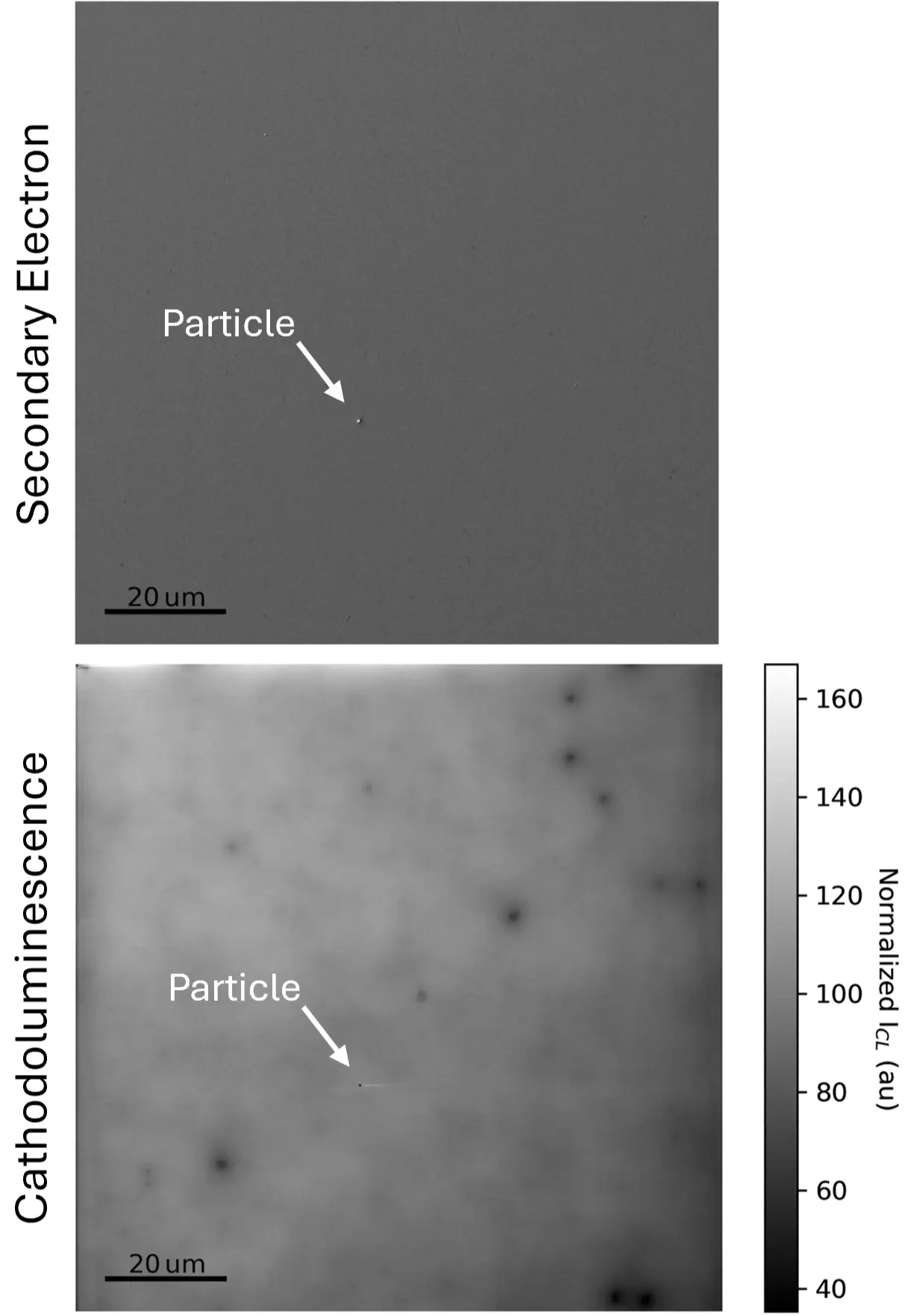
In the SE image, the only source of contrast is the presence of a small surface particle, which can also be seen in the CL map. The CL map, on the other hand, is much richer in contrast, featuring dark spots corresponding to TDs present at the material’s critical surface. The variation in the observed diameter of the TDs is linked to a combination of different species of TDs (edge type, screw type, mixed) and local variation in the quality of the grown material.
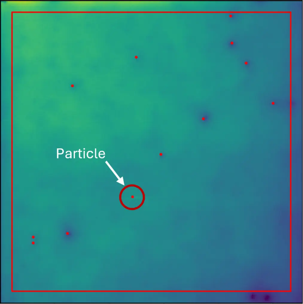
In this sample, the relative density of TDs makes counting them and performing statistics very simple, as shown in Figure 2. In the observed FOV, there are 11 real TDs (plus one false positive, caused by the particle, which is excluded), corresponding to an approximate density of 1.2 * 105 TDs/cm2. For epi layers which may be more or less defective, the FOV and number of frames acquired can be adapted to ensure statistical significance.
Crucially, many CL microscopes use parabolic light collection optics, which are not able to efficiently collect light over a large surface area. This limits their effective FOV to a couple of tens of micrometers or less and makes quantitative comparisons across the FOV impossible. With Attolight’s fully-integrated CL imaging objective, FOVs of a few hundred micrometers are possible with a uniform collection efficiency, allowing for much faster and more quantitative inspection over larger areas.
Conclusion
The exceptional resolving power of CL exceeds the capabilities of any other technique to identify threading dislocations in InP and related materials. The detection process is well-suited to automation and the sampling rate can be adapted to the volume of wafers to be inspected. Although this application note has only presented results after epitaxy and before device patterning, the process can equally be applied to substrate and device inspection. The integrated CL optics used by Attolight facilitate this by enabling a large FOV and quantitative comparison of results, allowing for much higher inspection throughput. Thus, CL is well-positioned to give manufacturers the ability to catch reliability-killing defects in their InP co-packaged optics before their devices fail in the field, saving them costly downtime and repair costs. Ultimately, CL will also be a valuable tool for tracing the origin of such defects and modifying the process flow to reduce or eliminate them.


More applications
.webp)
Resolving Picosecond Carrier Dynamics at the Nanoscale — The Attolight Allalin Chronos TRCL Solution
Identifying Atomic-Scale Defects Responsible for Blue Emission in hBN Using Correlative STEM-CL

Quantitative CL Uniquely Resolves Individual Point Defects in InGaN/GaN Quantum Wells, Solving Efficiency Gain Riddle
.webp)
Cathodoluminescence Analysis of Extra-Cellular Matrix
CL from Beam-Sensitive Optoelectronic Materials - Hybrid Halide Perovskites