Identifying Atomic-Scale Defects Responsible for Blue Emission in hBN Using Correlative STEM-CL
Precisely determining the source of a specific luminescence wavelength in a material helps to understand the physics of its band structure. In hexagonal boron nitride, beyond the expected UV emission at ~320 nm, folded trilayers also exhibit localized blue emission near 440 nm. Hyperspectral CL mapping identifies single-point emitters at this wavelength with sub-nanometer precision, while correlative high-angle annular dark-field (HAADF) imaging and electron energy loss spectroscopy (EELS) link the emission to carbon impurities in specific atomic columns. Modelling and density functional theory (DFT) confirm that the defect corresponds to a vertically aligned carbon dimer. These results highlight STEM-CL as a powerful method to pinpoint the structural and chemical origin of individual quantum emitters, offering insights that are critical for the future design and engineering of defect-based light sources. Importantly, the combination of high spatial and spectral resolution with unmatched collection efficiency in the Attolight Mönch STEM-CL system makes such correlative measurements possible.
The true power of modern TEMs comes not just from their subatomic spatial resolution, but rather the ability to harness this resolution to spatially correlate multiple distinct signals containing complementary information about the sample being investigated. In this application note, cathodoluminescence (CL) is introduced as a key correlative STEM technique for understanding the origin and nature of quantum emitters, specifically in folded multilayers of hexagonal boron nitride (hBN). All of the data presented in this application note is reproduced from H. Hou et al. [1]
hBN is known to emit in the UV (~320 nm), and the intensity of the CL emission is shown to be enhanced when the hBN is folded onto itself in a trilayer. In addition to the UV emission, folded hBN layers can exhibit localized blue emission at around 440 nm.
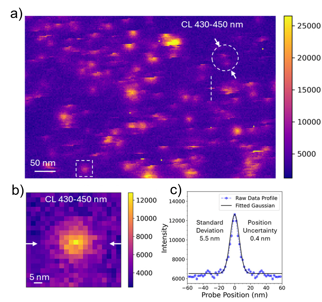
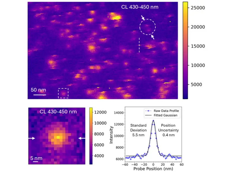
To investigate the origin of this localized blue emission, an overview CL hyperspectral map of a folded hBN flake was acquired to identify the location of individual emitters. Figure 1a shows such a map where CL intensity is integrated over the 430-450nm wavelength range, and in which both clusters and single point emitters can be observed. Figure 1b shows a higher-magnification CL map of one single-point emitter, as indicated by the dashed white box in the overview map. The emission profile appears to be highly localized and Gaussian in nature. Figure 1c shows an intensity profile cut along the center of another, similar single-point emitter, along with a corresponding Gaussian fit. Notably, the Gaussian profile has a standard deviation of 5.5 nm, a measure of the highly localized nature of the emission. A position uncertainty of only 0.4 nm also demonstrates that, for such emitters, CL benefits fully from the excellent spatial resolution of the STEM probe and that CL spectra can be correlated to other spatially-mapped properties with a high degree of confidence.
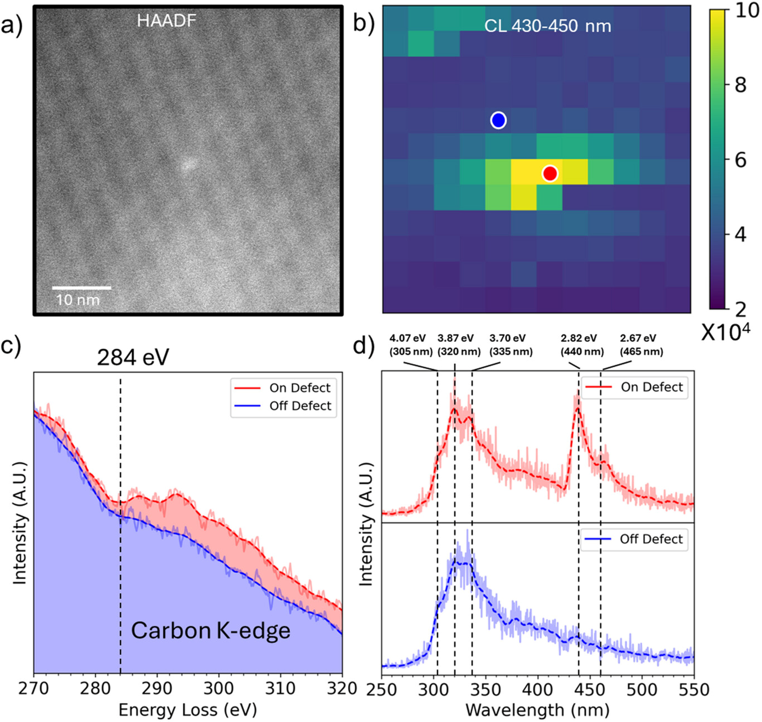
To understand more about the origin of blue emission in these samples, atomic resolution HAADF imaging was done at the site of individual emitters, as shown in Figure 2a,b. The HAADF image shows increased contrast at one atomic site at the center of the emission profile, indicating either a thickness or elemental composition difference at the location of that singular atomic column.
To gain further insight into the cause of the emission, electron energy loss spectroscopy (EELS) was performed directly at the central point of emission and a few nanometers away, as shown in Figure 2c. Looking at the spectral region around the carbon K-edge, it was revealed that a weak carbon signal is present at the center of the emitter, whereas no carbon was detected at the point away from the emitter. To confirm the correlation of the presence of carbon with the emission, two CL spectra were taken from the same points as the EELS spectra, which clearly show that, where carbon is detected, blue emission is also detected, whereas if no carbon is detected, no blue emission is observed. Thus, the blue emission in CL can be spatially correlated with a high degree of certainty to the presence of one or more carbon atoms which are situated in a single atomic column within the sample.
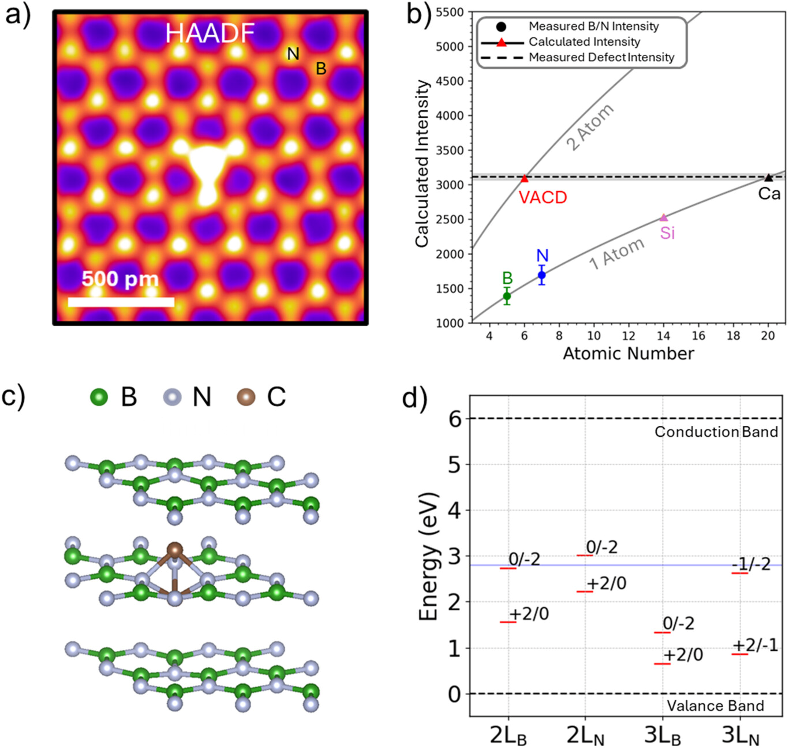
To determine more exactly the nature of the carbon impurity that is at the origin of the blue emission, high resolution HAADF imaging was performed on a different, thinner sample, allowing for better Z contrast imaging, as shown in Figure 3a. In this image, the HAADF intensity at the defect is clearly visible, and it can be determined that the defect lies in the atomic column normally occupied by boron atoms. Through modeling, shown in Figure 3b, it can be determined that the observed HAADF intensity closely matches what is expected for a vertically aligned carbon dimer (VACD), like what can be visualized in Figure 3c. Finally, density functional theory (DFT) was used to model the stability and defect energy level of various configurations of VACDs in multilayer hBN, as shown in Figure 3d. It is found that several of these defect configurations give rise to electronic states with energies close to those observed in CL and which are predicted to be stable due to their defect formation energies.
Thus, correlative STEM-CL was used in this study to identify individual quantum emitters in a multilayer hBN system, correlate their blue emission to HAADF contrast in a single atomic column, and help identify the origin of the emission as a defect created by a vertically aligned carbon dimer using EELS. Such correlative measurements are at the heart of what makes modern TEMs powerful tools for studying materials properties and demonstrate how STEM-CL helps to open a path toward understanding and engineering quantum emitters for advanced applications. Such insights would not be possible without the excellent spatial and spectral resolution and unmatched collection efficiency of the Attolight Mönch STEM-CL system.
Conclusion
The Attolight Mönch STEM-CL system provides the unmatched combination of field of view, spectral resolution, ease of use, and compatibility with other STEM techniques and specialized holders that enables the kind of advanced correlative studies presented here, driving innovation in the field of quantum emitters and beyond.
- H. Hou, M. Hua, V. S. C. Kolluru, W.-Y. Chen, K. Yin, P. Tripathi, M. K. Chan, B. T. Diroll, T. E. Gage, J.-M. Zuo, J. Wen, Nanometer Resolution Structure-Emission Correlation of Individual Quantum Emitters via Enhanced Cathodoluminescence in Twisted Hexagonal Boron Nitride. Adv. Mater. 2025, e01611. https://doi.org/10.1002/adma.202501611

More applications

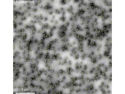
Quantitative CL Uniquely Resolves Individual Point Defects in InGaN/GaN Quantum Wells, Solving Efficiency Gain Riddle
.webp)
Cathodoluminescence Analysis of Extra-Cellular Matrix
CL from Beam-Sensitive Optoelectronic Materials - Hybrid Halide Perovskites
Applications on Defect Visualization and Counting in Optoelectronic Materials
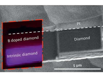
Applications on Semiconducting Diamond
