Background moutain Attolight
Säntis 300

Full Wafer Cathodoluminescence Microscope

The Säntis 300 is an automated process control system for wafers up to 300 mm, offering large field-of-view, fast scanning, and simultaneous SEM imaging and CL spectra acquisition.

Dashboard mockup
Characteristics

About our Full Wafer Cathodoluminescence-SEM Equipment

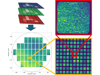
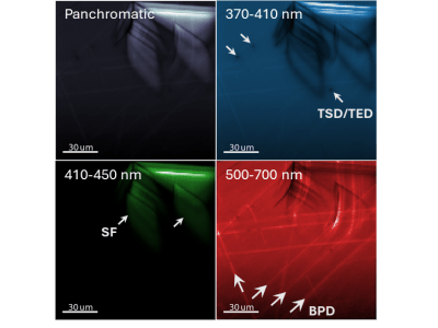
The system's quantitative CL technology offers unparalleled speed, accuracy, and repeatability with a large 300 μm field of view. Multiple acquisition modes enable detailed defect analysis, material inhomogeneity mapping, and dynamic process tracking, such as dopant activation or elemental fluctuations.

Small-diameter wafers and miscellaneously-shaped substrates can be manually affixed to larger susceptors for automated handling by the tool, making the Säntis 300 well-suited to failure analysis and research applications where quick turnaround time is important.

Dashboard mockup
Features

About our Full Wafer Cathodoluminescence Microscope

The standard Säntis 300 configuration includes a top-loading loadlock into which wafers are manually placed using a wafer wand. The loadlock facilitates quick loading and unloading operations, increasing throughput compared to our Allalin system. The tool can be upgraded to include support for wafer cassettes (FOUPs) or even a full EFEM with automated wafer handling for integration in fully-automated fabs.

  • Fully automated quantitativeCL metrology
  • Simultaneous SEM imaging & spectra acquisition
  • High throughput & automated wafer handling
  • Wafer bow mapping & alignment
  • Loadlock for fast sample exchange
  • Loadlock for rapid sample loading and unloading

System Configurations: Includes manual or automated loading options for enhanced throughput, with potential upgrades for full automation. It is optimized for cleanroom environments and equipped with height mapping sensors to maintain precision during measurements.

Trusted by top semiconductor companies and prestigious research institutes worldwide

Applications

Related Applications Using the Säntis 300

Discover how the Allalin platform can support your research.

Text Link
Process development
Text Link
Materials Science
Text Link
Micro/Nanowire
Text Link
GaN device
Text Link
Power electronics
Text Link
Life Science
Text Link
Optoelectronics

Scientific references

Heterotwin Zn3P2 superlattice nanowires: the role of indium insertion in the superlattice formation mechanism and their optical properties S. Escobar Steinvall, L. Ghisalberti, R. R. Zamani, N. Tappy, F. S. Hage, E. Stutz, M. Zamani, R. Paul, J.-B. Leran, Q. M. Ramasse, W. C. Carter, A. Fontcuberta i Morral arXiv preprint arXiv:2009.01533, 2020 2020
Efficient light-emitting diodes from mixed-dimensional perovskites on a fluoride interface B. Zhao, Y. Lian, L. Cui, G. Divitini, G. Kusch, E. Ruggeri, F. Auras, W. Li, D. Yang, B. Zhu, R. A. Oliver, J. L. MacManus-Driscoll, S. D. Stranks, D. Di, R. H. Friend Nature Electronics, 2020 2020
InGaN Quantum Dots Studied by Correlative Microscopy Techniques for Enhanced Light-Emitting Diodes I. Dimkou, E. Di Russo, P. Dalapati, J. Houard, N. Rochat, D. Cooper, E. Bellet-Amarlic, A. Grenier, E. Monroy, L. Rigutti ACS Applied Nano Materials, 3, 10, 10133–10143, 2020 2020
Continuous and Time-Resolved Cathodoluminescence Studies of Electron Injection Induced Effects in Gallium Nitride S. Modak, L. Chernyak, I. Lubomirsky, S. Khodorov In: Palestini C. (eds), Advanced Technologies for Security Applications. NATO Science for Peace and Security Series B: Physics and Biophysics, Springer, Dordrecht, 2020 2020

Scientific references

Combining in situ micro-photoluminescence and cathodoluminescence to understand defects photophysics in nanodiamonds BONNET, Noemie, TREUSSART, Francois, CHANG, Huan, et al. Microscopy and Microanalysis, 2021, vol. 27, no S1, p. 2104-2106 2021
Unveiling nanoscale optical and structural properties of TMD monolayers using combined electron spectroscopies BONNET, Noemie, LEE, Hae Yeon, FUHUI, S. H. A. O., et al. Microscopy and Microanalysis, 2021, vol. 27, no S1, p. 124-127 2021
Liquid-phase sintering of lead halide perovskites and metal-organic framework glasses Hou J, Chen P, Shukla A, Krajnc A, Wang T, Li X, Doasa R, Tizei LHG, Chan B, Johnstone DN, Lin R, Schülli TU, Martens I, Appadoo D, Ari MS, Wang Z, Wei T, Lo SC, Lu M, Li S, Namdas EB, Mali G, Cheetham AK, Collins SM, Chen V, Wang L, Bennett TD Science, 2021 Oct 29;374(6567):621-625 2021
Nanoscale modification of WS2 trion emission by its local electromagnetic environment BONNET, N., LEE, H.Y., SHAO, F., WOO, S.Y., BLAZIT, J.-D., WATANABE, K., TANIGUCHI, T., ZOBELLI, A., STEPHAN, O., KOCIACK, M., GRADECAK-GARAJ, S., TIZEI, L.H.G. Nano Lett., 2021, 21, 24, 10178–10185 2021

Ready to revolutionize your materials characterization approach?

Get in touch with us today to discover how our state-of-the-art cathodoluminescence tools can elevate your research and industry applications.
Already more than 30 systems installed globally!