Resolving Individual Quantum Emitters in GaN-AlN Superlattice Nanowires
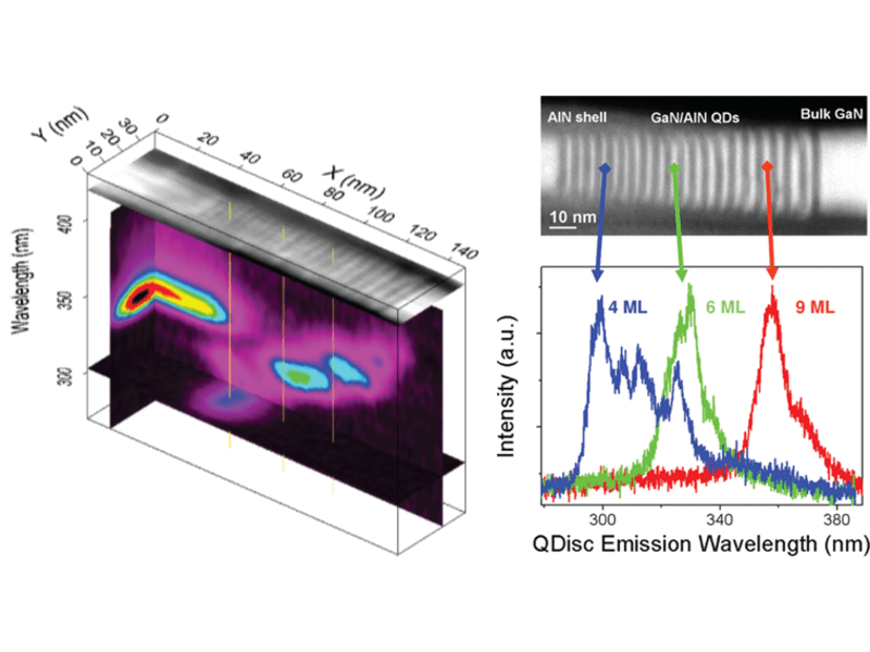
Stacks of GaN-AlN quantum discs (QDiscs) are a highly-tunable platform for photonic and optoelectronic applications, but until recently were only able to be optically characterized in ensembles due to their nanoscale dimensions and close proximity to one another. CL-STEM, however, unlocks the capability to spatially and spectrally resolve individual QDiscs down to just a few nanometers in dimensions. In this application note, we first present how this ability of CL-STEM is used to uncover the unintentional presence of quantum rods embedded in the QDisc sidewall. We then show how the excellent resolution of CL-STEM provides insight into the fundamental physics governing QDisc emission, including the effects of thickness, strain, and the quantum confined Stark effect.
Semiconductor nanowires (NWs) are an ideal platform to create quantum photonic and optoelectronic systems thanks to the many ways that they can be engineered in terms of size, composition and morphology. III-nitride NW heterostructures are of special interest due to their strong and tunable emission spanning the ultraviolet, visible and near infrared spectral range. However, their nanoscale dimensions present unique challenges for optical characterization. Traditional approaches, such as photoluminescence (PL) or near-field optical microscopy are diffraction-limited, making it impossible to address individual quantum components in a tightly packed ensemble.
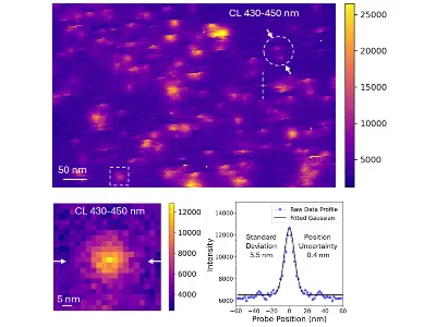
Cathodoluminescence spectroscopy in scanning transmission electron microscopy (CL-STEM) overcomes this limitation by using an electron beam probe which can be focused to sub-nanometer sizes to excite the sample. For bulk semiconductor systems, the spatial resolution in CL is often determined by the minority carrier diffusion length, which can be microns. However, in nanoscale heterogeneous materials systems, quantum confinement can be exploited to reduce the spatial extent of the luminescence to mere nanometers.
Figure 1 shows a typical setup for CL-STEM, which includes the standard components for STEM, including a HAADF detector for electron diffraction contrast imaging, as well as a retractable mirror and corresponding light spectrometer for collecting and analyzing cathodoluminescence from the sample. Figure 1 also shows an example HAADF and CL hyperspectral image for a GaN-AlN superlattice NW featuring quantum discs (QDiscs) formed by the inclusion of periodic AlN barrier layers during growth.
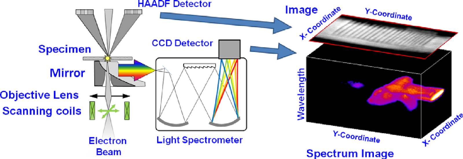
The CL hyperspectral image consists of an information-rich 3D data cube, with two spatial dimensions and one wavelength dimension. In this representation, spectral features can be correlated to structural features of the NW. In the example shown in Figure 1, the NW has a rich spatial-spectral structure that is mostly contiguous across all dimensions but includes one feature which is both spatially and spectrally isolated from the rest. Correlating this feature with the HAADF image reveals its origin to be a GaN quantum rod (QRod) which was unintentionally grown into the sidewall of the NW.
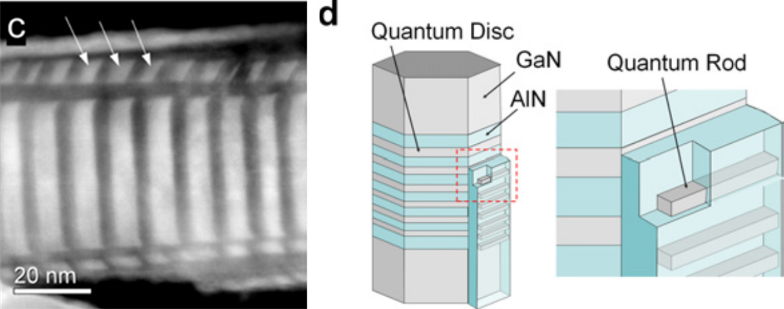
Figure 2 shows a HAADF image and schematic representation visualizing the presence of a QRod grown into the sidewall of the NW. The formation of the QRod during NW growth was unintentional and leads to emission that is spatially and spectrally distinct when observed by CL-STEM.
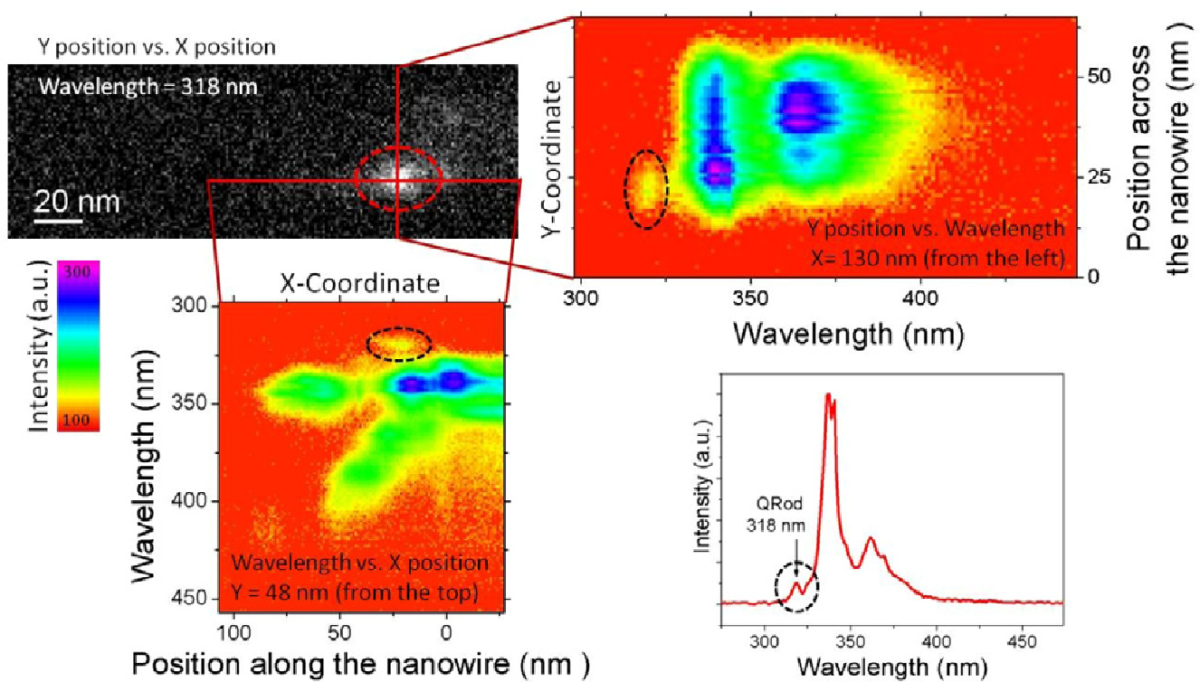
Figure 3 gives a more detailed look at how this distinct QRod emission can be visualized and characterized using CL-STEM hyperspectral mapping. Filtering the CL image for the wavelength that corresponds to the QRod (318 ± 4 nm), one can identify a single bright spot in the field of view. Taking spatial-spectral slices through this location in the hyperspectral data cube, one can create plots that map the emission spectrum as a function of position along both the x and y axes. In these views, the QRod emission is clearly discernible at shorter wavelengths than the QDiscs due to their smaller size and therefore stronger confinement. The QRod emission intensity is also less than that of the QDiscs due to the relatively small volume fraction that the QRods represent. Notably, in the spatial-spectral slices shown in Figure 3 one begins to see hints that individual QDiscs can be resolved by CL-STEM.
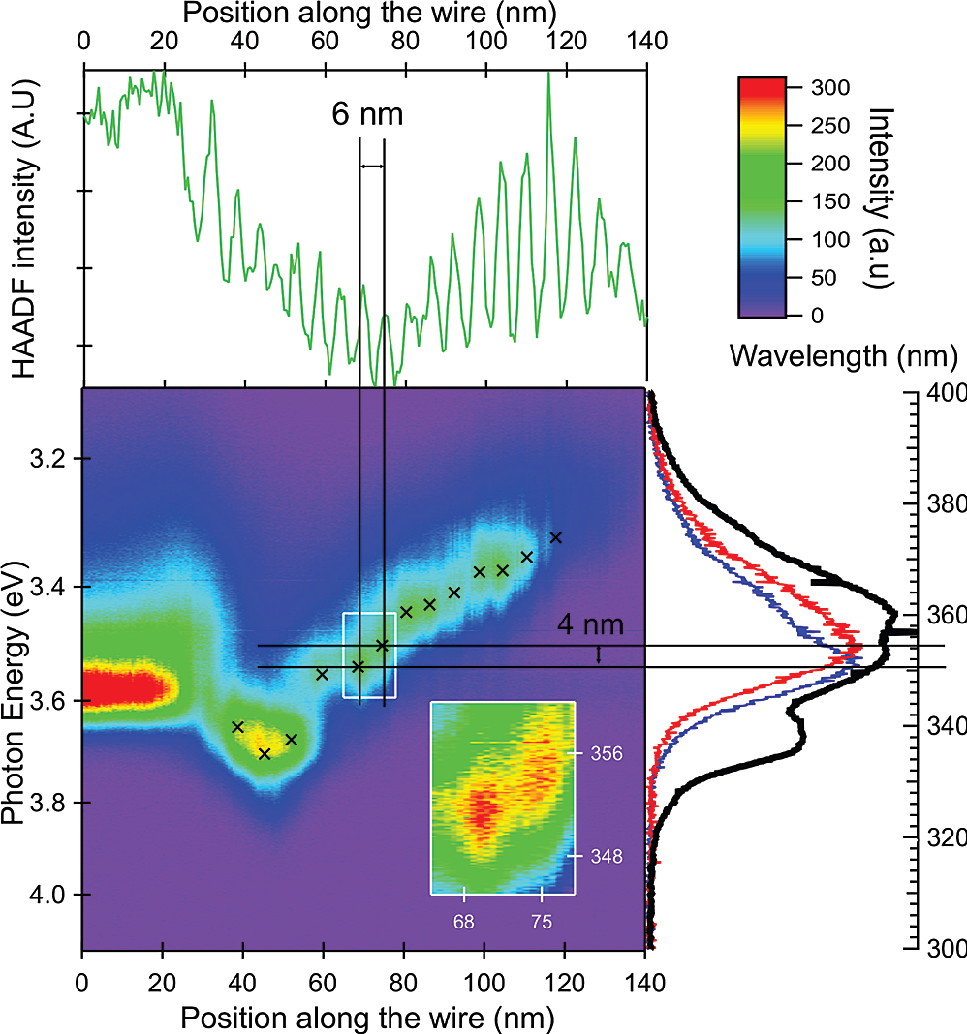
In a related study, the authors correlate contrast in the HAADF image with intensity peaks in the CL signal in order to resolve individual QDiscs which were fabricated with varying thicknesses. Shown in Figure 4, one observes fluctuations in the HAADF intensity as a function of position along the nanowire. Peaks in HAADF intensity correspond to GaN layers, which scatter electrons more than AlN layers. The location of the QDiscs as identified by HAADF contrast can be exactly matched to peaks in the CL intensity, thereby resolving the unique spectral features of individual QDiscs. What’s more, because the GaN-AlN superlattice was grown with varying layer thicknesses along the length of the NW, the peak emission wavelength of each QDisc can be used to quantify its thickness; thicker QDiscs emit at longer wavelengths. This is seen in Figure 4 as a gradual increase in emission wavelength (decrease in photon energy) as one moves from the 60 nm position in the NW toward the 120 nm position. Figure 4 illustrates both the spatial and spectral resolution of two neighboring QDiscs, shown in the inset, which have a spatial separation of 6 nm and a spectral separation of 4 nm. The ability to resolve these features far below the minority carrier diffusion length is thanks to the high degree of quantum confinement inside the QDisc.
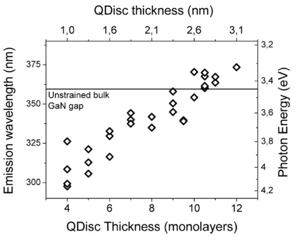
Using high-resolution HAADF-STEM imaging, the thickness of individual QDiscs was quantified with monolayer precision and correlated to their emission wavelength. Figure 5 shows the strong linear correlation between QDisc thickness and emission wavelength. Interestingly, many of the QDiscs emit at photon energies below the bulk GaN band gap, an effect that is attributed to the quantum-confined Stark effect. Additionally, the authors attribute the spread in photon energy for QDiscs of the exact same thickness to differences in strain states depending on the position of the QDisc in the NW. This correlated HAADF-CL-STEM study offers important insights into the multitude of factors that influence the emission properties of quantum emitters in an ensemble, a feat which would not be possible by all-optical techniques or by electron energy loss spectroscopy (EELS).
The results presented in this application note were obtained using a predecessor to the Mönch CL-STEM system, which has since been further refined for more robust and repeatable operation. Such results demonstrate the power of CL-STEM to advance the understanding of quantum mechanical systems at a scale that is inaccessible with all-optical techniques. This is invaluable for identifying contributions from undesired inclusions in the sample, as was the case for the QRods. The excellent spatial and spectral resolution are also key to uncovering the underlying physical phenomena, such as the QCSE and strain variation, governing the emission properties of the nanostructures. All in all, the Mönch system allows one to unlock the full potential of STEM to study the materials systems that will shape technologies of the future.
- L.F. Zagonel, L. Rigutti, M. Tchernycheva, G. Jacopin, R. Songmuang, and M. Kociak. Visualizing highly localized luminescence in GaN/AlN heterostructures in nanowires. Nanotechnology, vol. 23, no. 45, 2012. https://doi.org/10.1088/0957-4484/23/45/455205
- L.F. Zagonel, S. Mazzucco, M. Tencé, K. March, R. Bernard, B. Laslier, G. Jacopin, M. Tchernyvcheva, L. Rigutti, F.H. Julien, R. Songmuang, M. Kociak, Nanometer Scale Spectral Imaging of Quantum Emitters in Nanowires and Its Correlation to Their Atomically Resolved Structure. Nano Letters, vol. 11, no. 2, 2011. https://doi.org/10.1021/nl103549t



.webp)
