Correlating Structural and Optical Properties of Lead Halide Perovskites
Lead halide perovskites (LHPs) can be fabricated with excellent optoelectronic properties, but it is essential to understand the impact of their interface with the matrix in which they are embedded. To do this, their optical properties must be studied at a nanometer-scale spatial resolution, made possible using cathodoluminescence (CL) in a scanning transmission electron microscope (STEM). In this application note, we present how CL-STEM is used to attribute the optical characteristics of LHPs, such as emission wavelength and bandwidth, to structural properties such as grain size, composition and interface quality with the embedding matrix. These results are made possible by the Attolight Mönch system’s efficiency and compatibility with complementary techniques.
Lead halide perovskites (LHP) are a promising family of materials thanks to their outstanding optoelectronic properties, but suffer from several weaknesses, including difficulty controlling their crystal phase, instability in certain environments, and poor understanding of their interfaces. Their properties can be stabilized by fabricating the LHP inside of a glassy metal-organic framework (MOF) matrix via liquid-phase sintering, but understanding the impacts of alloy composition, interface effects and quantum confinement requires nanometer-scale characterization of their luminescence.
To accomplish this, cathodoluminescence scanning transmission electron microscopy (CL-STEM) can be used to correlate a material’s nanostructure with its emission properties. In combination with other STEM techniques, such as high-angle annular darkfield (HAADF) imaging and energy-dispersive x-ray spectroscopy (EDS), CL-STEM allows one to gain unprecedented insight into the interplay between LHP composition, grain size, and interactions with the embedding matrix.
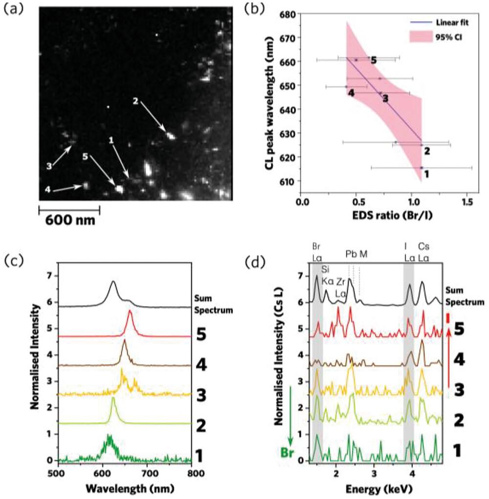
As an example, Figure 1 shows results from a study performed on CsPbBr1.5I1.5 embedded a MOF matrix in which different grains of the LHP exhibit varying emission wavelengths, ranging from 610 to 690 nm. To determine the origin of this wavelength variation, hyperspectral CL maps were acquired and overlayed with EDS maps to correlate the luminescence wavelength with the ratio of bromine and iodine ions, which affects the band gap energy of the material. Figure 1a presents the CL panchromatic map from the sample while Figure 1b plots the CL peak wavelength as a function of the Br/I ratio as extracted by EDS. Despite uncertainty in the measurements, there is a clear correlation between the stoichiometric variation in individual LHP grains and their emission wavelength. As the Br/I ratio increases, the emission wavelength decreases, which is due to the increase in band gap energy as larger iodine ions are substituted by smaller bromine ions. The individual CL and EDS spectra for each labeled grain in the LHP are shown in Figures 1c and d, respectively. [1]
This study was facilitated using the Attolight Mönch CL-STEM add-on system, which benefits from the sub-nm spatial resolution of STEM and the efficient Attolight light collection optics, providing the user ultimate flexibility and reliability in their experiments. With a retractable mirror that can move independently of the sample holder, the Mönch is both quick to align and compatible with other in-STEM techniques like EDS, making it an invaluable tool for detailed characterization of nanostructured materials.
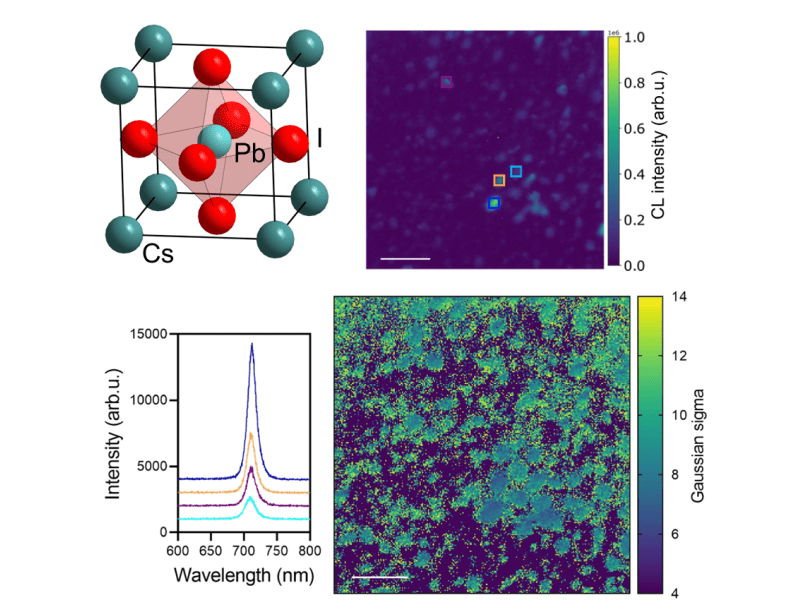
Another example of how CL-STEM can elucidate the phenomena governing the optical properties of LHPs is shown in Figure 2. Figure 2a shows a HAADF image of CsPbI3 embedded in a MOF matrix while Figure 2b gives a panchromatic CL intensity map of the same field of view. Figure 2c shows individual CL spectra from a few different LHP grains and Figure 2d shows the width of the emission peak (fitted as a gaussian, where σ corresponds to the standard deviation) at each pixel in the image. One quickly observes that there does not appear to be a correlation between grain size and emission intensity, which confirms that the emission intensity is not predominantly determined by quantum confinement effects. What’s more, the emission peak width appears to generally increase at the edge of the grains, which hints at the significant role played by the interface between the LHP and the MOF matrix. [2]
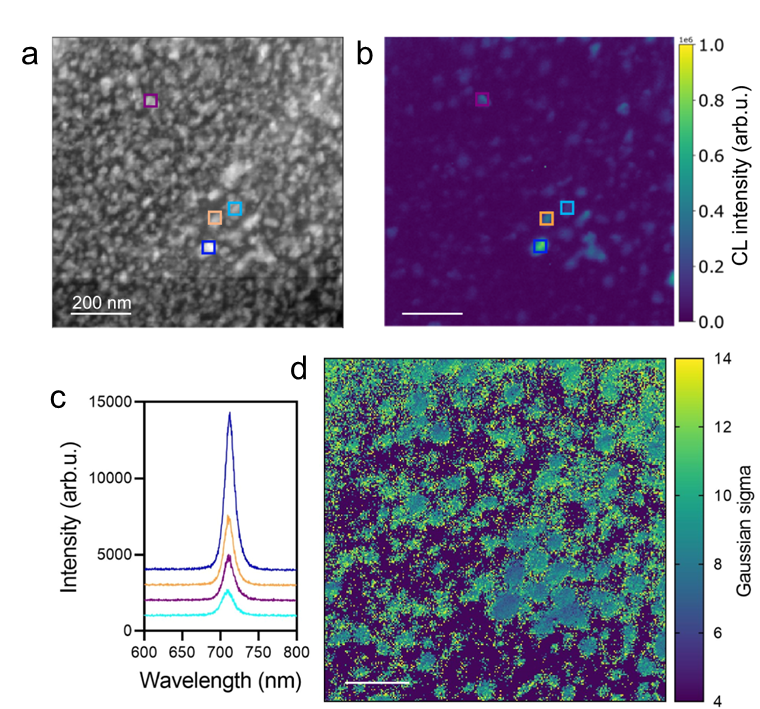
The authors then go on to correlate the results presented in Figure 2 with other analysis techniques, including electron energy loss spectroscopy (EELS), and perform sintering experiments at various temperatures. Through the synthesis of these results, they are able to conclude that the quality and stability of the CsPbI3 is ultimately determined by the quality of its interface with the MOF matrix.
By combining CL-STEM with other analysis techniques, the authors of both studies presented in this application note were able to gain unparalleled insight into the functional properties of their perovskite material system. This highlights the tremendous power of CL-STEM as a complementary technique to more traditional characterization methods. Thanks to its experimental flexibility and compatibility with other in-STEM techniques, including EDS and EELS, the Attolight Mönch CL system provides users with the best possible opportunity to detect and analyze all of the rich signals coming from their materials systems.
- M. Ghasemi, X. Li, C. Tang, et al. Effective Suppressing Phase Segregation of Mixed-Halide Perovskite by Glassy Metal-Organic Frameworks. Small, vol. 19, 2023. https://doi.org/10.1002/smll.202304236
- X. Li, W. Huang, A. Krajnc, et al. Interfacial alloying between lead halide perovskite crystals and hybrid glasses. Nat Communications, vol. 14, 2023. https://doi.org/10.1038/s41467-023-43247-6



.webp)
