
Cathodoluminescence spectroscopy
Introduction
Luminescence is generally defined as the emission of radiation from electronically excited matter. This definition excludes other radiation emission mechanisms such as incandescence and bremsstrahlung. For experimental reasons, luminescence is also typically restricted to radiation in the ultra-violet (UV)/visible/near-infrared (IR) range. Depending on the nature of the excitation source, luminescence is referred to as photoluminescence (PL) when photons are used as the excitation source, electroluminescence (EL) when an electrical current is used, chemiluminescence when a chemical reaction is used and finally cathodoluminescence (CL) when a high energy electron beam is used. When the light intensity from CL is measured with a point detector and plotted as a function of the electron beam position on the sample, the method is referred to as CL imaging. When the light is analysed as a function of its energy or wavelength, this is known as CL spectroscopy.
Principles
Within amorphous matter (a gas, a liquid or a glass), a UV, visible or near-IR photon may be emitted following the excitation of an electron from an outer atomic (valence) shell or a molecular orbital. Similarly, in a semiconducting or insulating crystalline solid, a UV, visible or near-IR photon may be emitted following the excitation of an electron from the valence band to the conduction band, leaving a hole in the valence band (Figure 1). Subsequently, the electron relaxes to the conduction band minimum (CBM), the hole to the valence band maximum (VBM), and they both diffuse in the material. Eventually, they recombine, and the energy E is released as light of frequency ν = Eh , where h is the Planck constant.
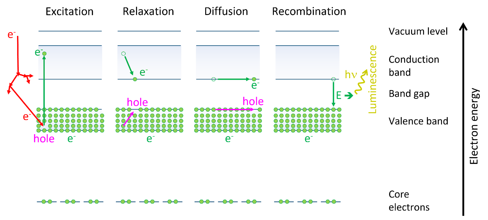
In addition to band-to-band recombination, there are other pathways for carriers to radiatively recombine inside of a material that are not discussed here for the sake of simplicity. In CL imaging, all radiative pathways contribute to the measured panchromatic light intensity. CL spectroscopy involves studying the intensity of the light emitted by a material as a function of its wavelength or energy. The result is a spectrum whose features can be correlated to radiative electronic transitions inside the sample to gain insight into the material’s properties.
Instrumentation
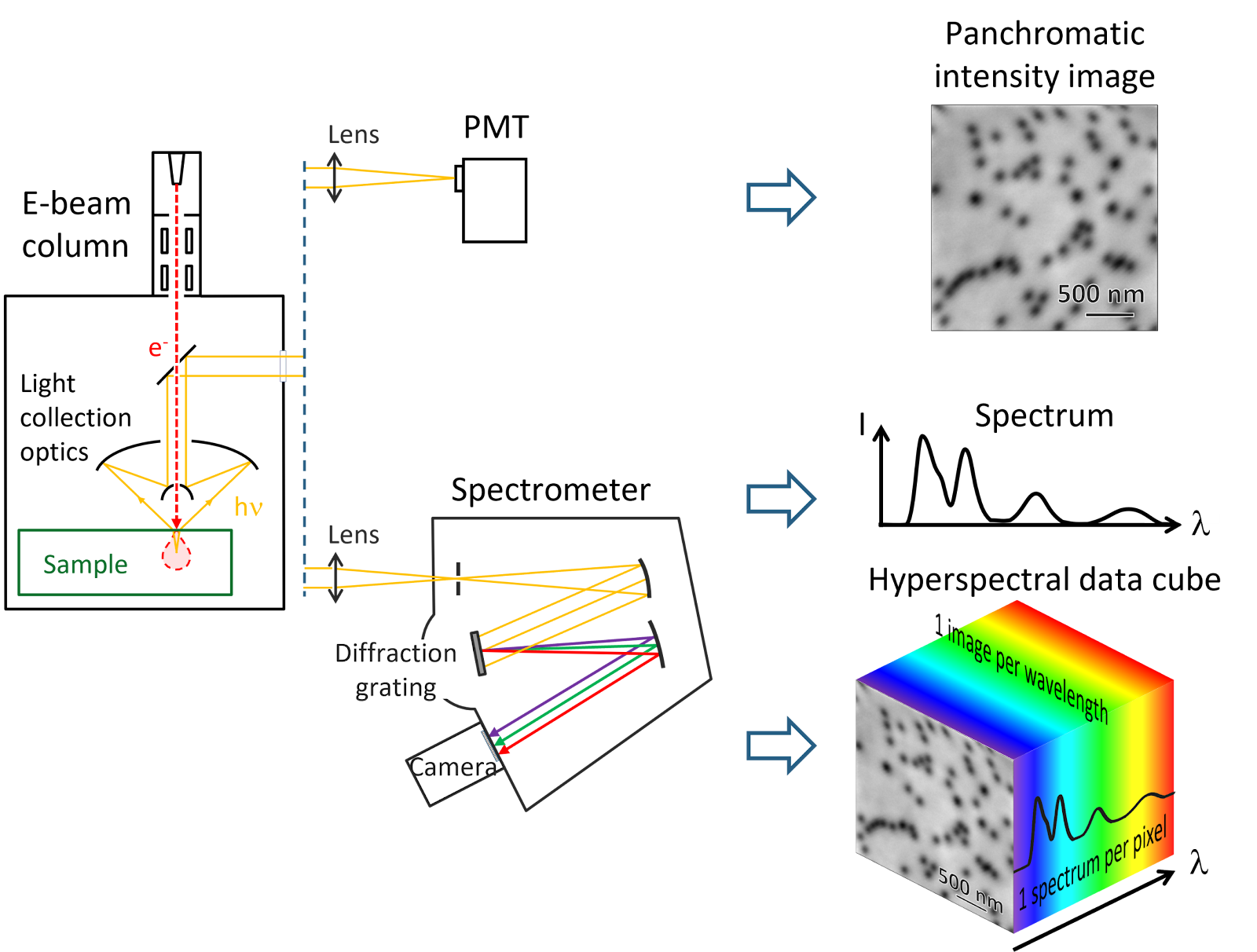
A typical setup for CL includes a scanning electron beam and a light collection system (Figure 2). The collected light can be captured by a point detector such as a photomultiplier tube (PMT) to obtain a panchromatic intensity image or analyzed with a spectrometer to obtain a spectrum or a hyperspectral data cube.
The voltage and the current of the primary electron beam can be tuned to adjust its penetration depth and the carrier generation rate in the sample. The diffraction grating inside the spectrometer can be selected to provide the desired wavelength range and optimum efficiency. Typically, a CCD camera is used to simultaneously record the intensity on a range of wavelengths.
Example results
Nanowire-based microLEDs
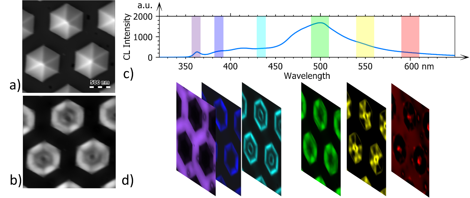
GaInN/GaN multiple quantum shell nanowire microLEDs are a contender for next generation display devices. Their luminescence can be characterized in detail using CL hyperspectral imaging (Figure 2). Simultaneously acquired secondary electron (SE) and panchromatic CL intensity images of the structures in top view are presented in Figure 2a and b. The emission spectrum averaged over the entire image is shown in Figure 2c. Integrating the emission intensity over various wavelength ranges (bands), typically around emission peaks, leads to different images (Figure 2d), called colorized band images, which can represent a specific material in the stack or a particular characteristic of one material. For further information, see Ref [1].
Horizontal nanowire
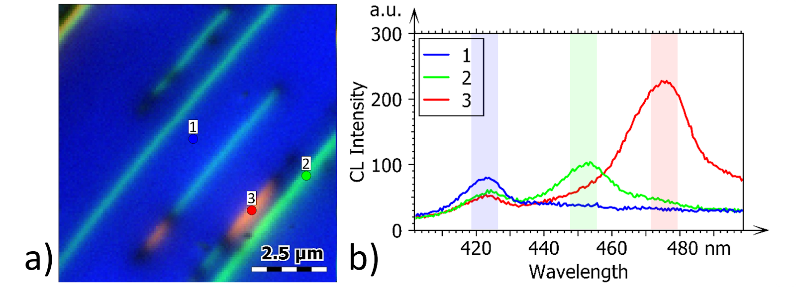
Figure 3b highlights two regions emitting at different wavelengths, or energies, within a horizontal quantum well nanowire. The emission spectra at the spots marked in Figure 3b are shown in Figure 3c, while the SE image acquired simultaneously is displayed in Figure 3a.

GaN on Si epitaxial stack
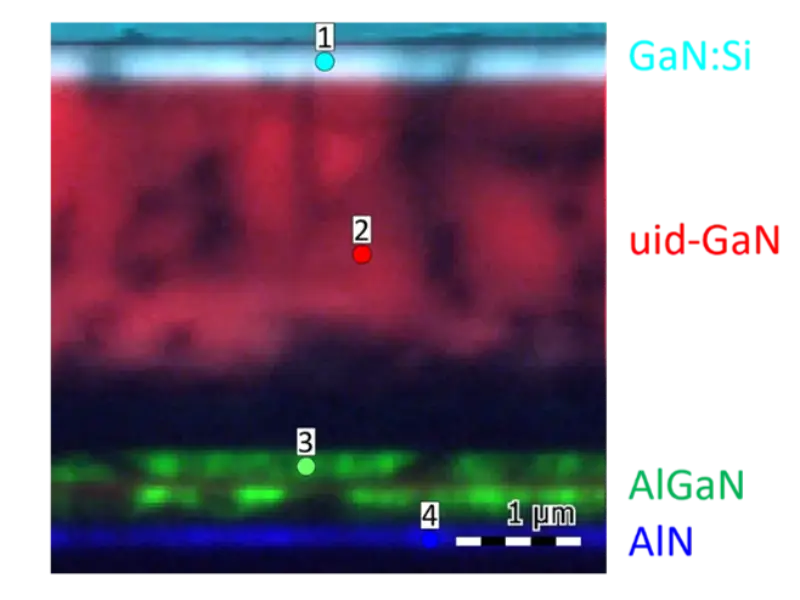
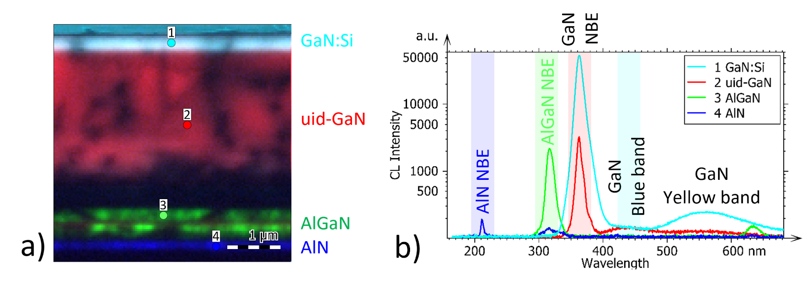
GaN on Si epitaxial stacks are used in various applications, including high-electron-mobility transistors (HEMT) for power devices. Figure 4 shows CL data acquired on the cross-section of such a stack. In Figure 4a, the images of the emission intensities integrated over the wavelength ranges shown in Figure 4b are colorized and superposed to obtain a single colorized bands image. The dark patterns are threading dislocations. Figure 4b presents the spectra emitted from the spots shown in Figure 4a. For further information on CL characterisation of HEMPT devices, see Ref [2].
Threading dislocations in GaN on Si
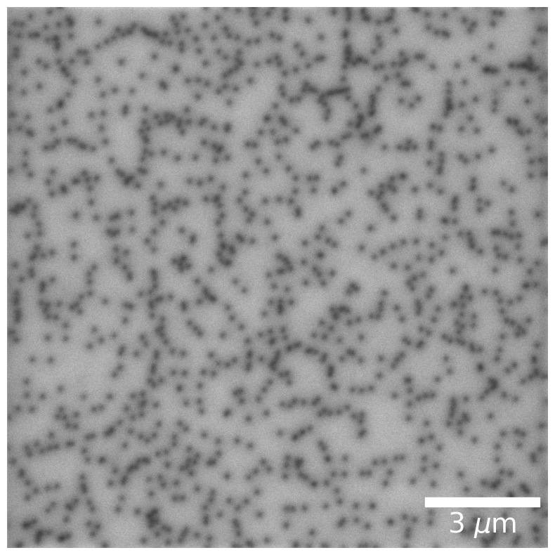
Threading dislocations (TDs) are one-dimensional extended crystallographic defects that arise at the interface with the substrate during heteroepitaxy and run roughly parallel to the growth direction. They manifest themselves as dark spots in CL panchromatic images because of an increased non-radiative recombination (NRR) rate near their core. In Figure 5 TDs with a density of 5.9×10⁻⁸ cm-2 are observed on a GaN on Si sample. More information can be found in Ref [3].
Stacking faults in SiC
Figure 6a shows stacking faults in cross-section within a grain of 6H-SiC powder. The stacking faults are delimited by dislocations, which appear as dark spots because of an increased non-radiative recombination rate (NRR) near their core. The emission wavelength from stacking faults is shifted compared with the emission from bulk 6H-SiC (Figure 6b).
Highly Mg-doped GaN
In Figure 7, the variation in emission spectrum (Figure 7b) denotes local variations (Figure 7a) in MgGa concentration within a layer of highly-doped GaN:Mg.
Perovskite layer
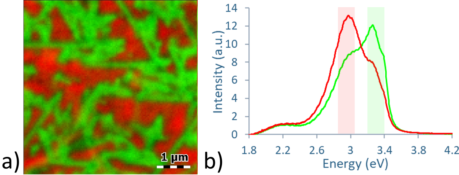
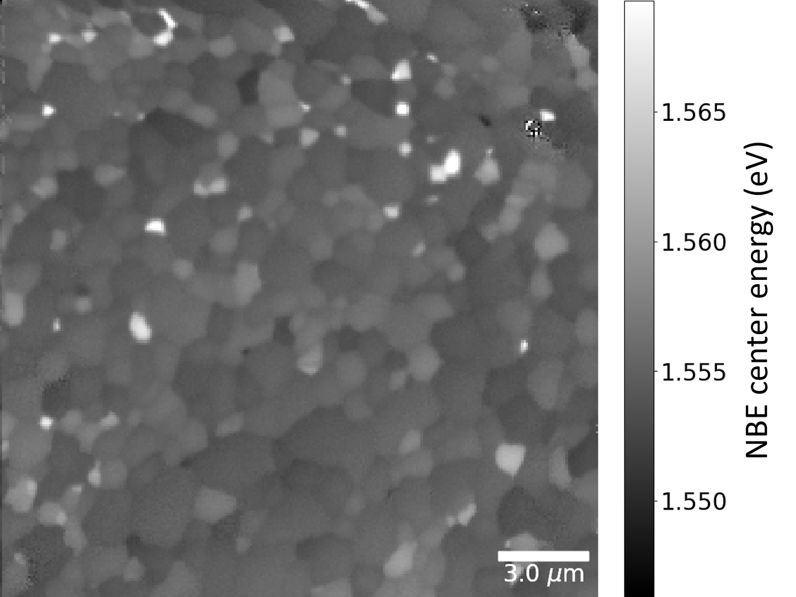
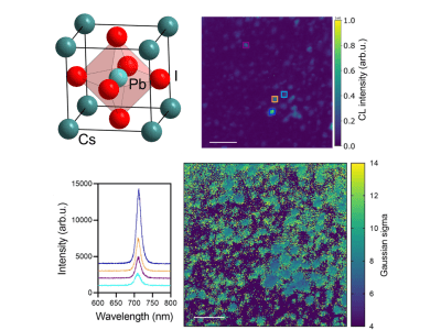
Some materials of perovskite structure have attracted interest because of their photovoltaic properties. Figure 8 evidences small variations in the centre energy of the near-band-edge (NBE) emission peak between the grains of a perovskite layer. For further information, see Refs [4] and [5].
Patterned plasmonic structures
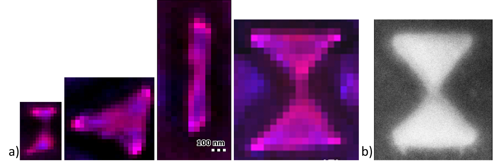
Figure 9 highlights variations in emission intensity and wavelengths within nanoscale TiN on Si structures of different shapes. The variations are due to quantum oscillations of the free electron cloud, or plasmons, within the metal.
α-MoO3 flakes
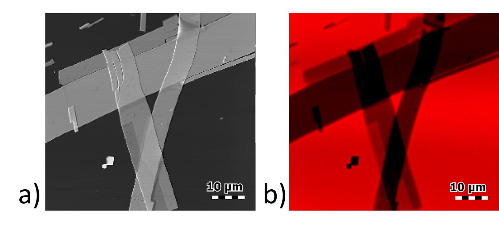
α-MoO3 is a wide-bandgap layered semiconductor. Figure 11a and b display simultaneously-acquired SE and CL images of MoO3 sheets superposed on a SiO2/Si substrate. In Figure 11b, the SiO2 luminescence around 650 nm is absorbed by the successive MoO3 layers, resulting in the observed contrast. A similar observation can be found in Ref [6].
Benefits and Further Reading
[1] S. Inaba, W. Lu, A. Shima, S. Ii, M. Takahashi, Y. Yamanaka, Y. Hattori, K. Kubota, K. Huang, M. Iwaya, T. Takeuchi, and S. Kamiyama, Phys. Status Solidi A 2024, 2400029. https://doi.org/10.1002/pssa.202400029
[2] C. Monachon, M. S. Zielinski, J. Berney, D. Poppitz, A. Graff, S. Breuer, L. Kirste, proceedings of IEEE IRPS 2018. https://ieeexplore.ieee.org/document/8353623
[3] M. Fouchier, C. Monachon, M. Davies, proceedings of ISFA 2023, p. 463-468.
https://doi.org/10.31399/asm.cp.istfa2023p0463
[4] C. Liu, Y. Yang, K. Rakstys, A. Mahata, M. Franckevicius, E. Mosconi, R. Skackauskaite, B. Ding, K. G. Brooks, O. J. Usiobo, J.-N. Audinot, H. Kanda, S. Driukas, G. Kavaliauskaite, V. Gulbinas, M. Dessimoz, V. Getautis, F. De Angelis, Y. Ding, S. Dai, P. J. Dyson and M. K. Nazeeruddin, Nat. Commun. 12, 6394 (2021). https://www.nature.com/articles/s41467-021-26754-2
[5] E. Shirzadi, N. Tappy, F. Ansari, M. K. Nazeeruddin, A. Hagfeldt and P. J. Dyson, Adv. Sci. 2022, 9, 2103729. https://doi.org/10.1002/advs.202103729
[6] M. Negri, L. Francaviglia, D. Dumcenco, M. Bosi, D. Kaplan, V. Swaminathan, G. Salviati, A. Kis, F. Fabbri, and A. Fontcuberta i Morral, Nano Lett. 20, 567−576 (2020). https://pubs.acs.org/doi/full/10.1021/acs.nanolett.9b04304#
Latest Scientific Publications
Cathodoluminescence spectroscopy
Resolving individual quantum emitters in GaN-AlN superlattice nanowires
Correlating structural and optical properties of lead halide perovskites
Explore our high-resolution cathodoluminescence tools designed for superior materials characterization.


