
In-SEM Raman Spectroscopy
Introduction
Raman spectroscopy is an analytical technique used to determine the vibrational modes of crystals and molecules, offering unique insights into their structural and chemical properties. The technique is based on the inelastic scattering of monochromatic light, typically from a laser, caused by molecular and lattice vibrations. When the light source interacts with a molecule or on? the surface of a solid, a small fraction of the light can undergo a shift in energy corresponding to vibrational energy levels of the sample. This is the Raman scattering process, named after the Indian physicist C.V. Raman who observed it first in 1928. Analyzing these energy shifts enables scientists to perform precise characterizations on a wide variety of samples.
Principles
In solid-state physics, Raman spectroscopy provides critical insights into the phonon modes, lattice dynamics, and crystal structure of solids. For semiconductors, superconductors, and nanomaterials, Raman helps to determine properties like stress, strain, and defects in crystal lattices. To a large extent, the advantages of Raman spectroscopy are identical to those of photoluminescence (PL). Raman spectroscopy is also non-destructive, sensitive, versatile and requires minimal sample preparation. The use cases, however, are mostly complementary. PL insights reach into functional properties of a material, related to electrical and optical properties. Raman information, on the other hand, is first and foremost structural. The process is illustrated below.
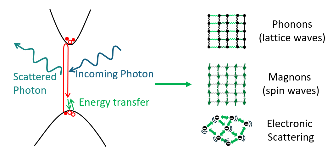
Quasiparticle states involved in Raman scattering are intrinsically linked to the laser wavelength used in the experiment. Unlike photoluminescence, where photons are emitted at a fixed energy regardless of the excitation wavelength, Raman scattering creates a spectrum with peaks at fixed energy differences with respect to the laser source.
The axis commonly used to represent Raman spectra, commonly called Raman shift, is measured in relative inverse centimetres, measured with respect to the laser wavelength. Its relationship with the wavelength is the following:

In a scanning electron microscope (SEM), Raman spectroscopy can be performed alongside high-resolution imaging and other in-situ techniques, which enables a large variety of in-situ and correlative studies. Advanced Raman experiments involve mapping samples to obtain spatially resolved information, and varying the laser polarization to selectively excite specific phonon modes in a sample.
Instrumentation
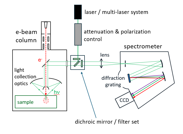
The instrumentation needed to perform Raman spectroscopy is nearly identical to that of PL spectroscopy. However, spectral filtering components and spectrometer need to be specifically fitted for the technique. The typical range of useful Raman shifts extends from 200 to 3000 cm-1. In wavelengths terms, this translates approximately to 538-633 nm relative to a laser wavelength of 532 nm. Raman is thus a relatively high resolution spectroscopy technique.
Additionally, if PL efficiency can reach up to a few percent of laser power, Raman excitation efficiencies range from 10-6 to 10-4 depending on sample and laser wavelength. Rejection of laser wavelength must thus be extremely efficient as well. In the Allalin platform, the spectroscopy setup sketched below can be easily adapted to Raman / PL experiment by choosing appropriate dichroic filter sets and spectrometer gratings. The system is designed to provide alignment-free swapping of optical elements, ensuring optimal PL and Raman performances at all times.
Example results
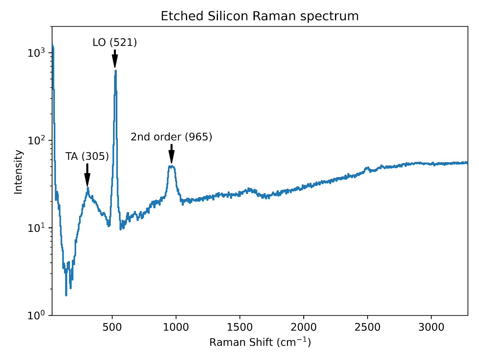
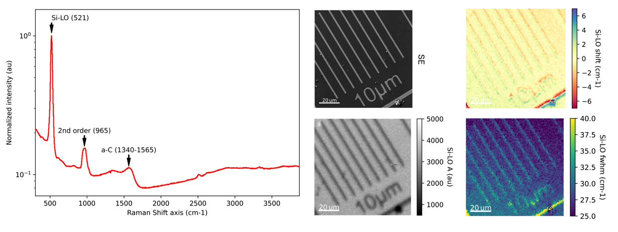
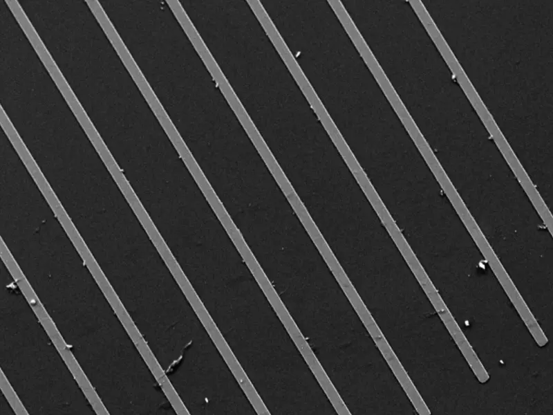
Figure 3 shows the Raman spectrum of etched silicon. Hyperspectral image analysis is used to obtain Figure 4 form it by fitting subpeaks on each of the peaks indicated. The image showns is that of a polysilicon-on-Si calibration grid, showing a resolution well below 10 µm.
Benefits and Further Reading
- Ian R.L. and Edwards H.G.M. (editors), Handbook of Raman Spectroscopy, CRC Press, 2001. ISBN: 9780824705572
- Smith E and Dent G, Modern Raman Spectroscopy: A Practical Approach (2nd edition), Wiley, 2019. ISBN: 9781119440550
References
- Parker, J. H., D. W. Feldman, and M. Ashkin. “Raman Scattering by Silicon and Germanium.” Physical Review 155, no. 3 (March 15, 1967): 712–14. https://doi.org/10.1103/PhysRev.155.712.
- Milani, Alberto, Matteo Tommasini, Valeria Russo, Andrea Li Bassi, Andrea Lucotti, Franco Cataldo, and Carlo S. Casari. “Raman Spectroscopy as a Tool to Investigate the Structure and Electronic Properties of Carbon-Atom Wires.” Beilstein Journal of Nanotechnology 6, no. 1 (February 17, 2015): 480–91. https://doi.org/10.3762/bjnano.6.49.
Latest Scientific Publications
Explore our high-resolution cathodoluminescence tools designed for superior materials characterization.

