
EBIC/EBAC imaging
Introduction
Electron beam induced current (EBIC) and electron beam absorbed current (EBAC) are imaging techniques that can be employed in an electron microscope in addition to secondary electron (SE) and backscattered electron (BSE) imaging. EBAC reveals current pathways through the sample as image contrast. It is used to detect short circuits and broken connections in electrical devices. Similarly, EBIC shows electric fields in a sample and is principally used to characterize semiconductor junctions. Both require electrical connection(s) to the sample and benefit from a nanoprobing solution to harness their full potential.
Principles
In electron microscopy, the balance between sample irradiation, SE emission and backscattering creates a net absorbed charge in the sample, either positive or negative. Sample grounding is essential for this reason, as the specimen-absorbed charge and associated current must find a path to ground in order to prevent sample charging. The core idea of EBAC imaging is to place a current sensing device in the grounding path of specimen current, so that specimen current variations can be imaged as the beam is scanned on the sample.
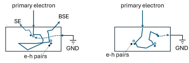
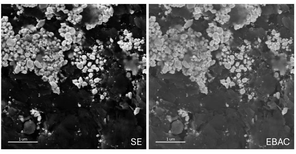
In the simplest EBAC implementation, specimen current is indiscriminately collected on the whole sample. Contrast occurs through modulation of the SE yield with sample topography and materials. In that case, EBAC images are fairly similar to SE, although they present the advantages of avoiding screening effects and non-linearity artifacts that sometimes occur with SE detectors.
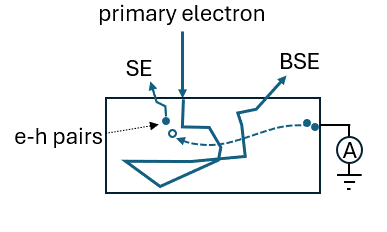
Another, and perhaps the best-known, EBAC imaging mode is also called Resistive Contrast Imaging (RCI). The sample is grounded separately from the current sensing path, which is wired to a high-conduction region of the sample, typically the interconnects of an electronic chip. Competing paths to ground for the specimen current (through the measurement device or not) allow to image electrical continuity in the sample at the nanoscale and detect defects in buried conductive layers.
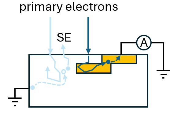
Finally, when an electric field is present in a sample, typically a semiconductor bipolar or Schottky junction, electron beam induced current (EBIC) can occur. Electron-hole pairs generated by the primary electron beam get separated by the field and collected on the competing grounds on both sides of the junction. At the junction, a large current amplification occurs, and the collected signal no longer depends on secondary electron/backscattering yield. Contrast directly depends on electric field intensity and can be linked back to the material’s properties such as doping concentration or carrier mobilities.
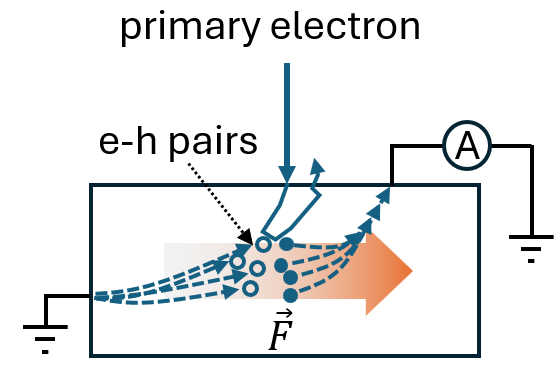
The abovementioned configurations provide an overview of basic EBIC/EBAC imaging in scanning electron microscopy. In advanced utilisations of the technique, it might be useful to apply bias voltages and currents to the sample. For example, in EBIC measurements, applying voltage to a junction can dramatically modulate electric field inside the sample, allowing to study, among other things, breakdown effects and field spatial repartition in semiconductor devices under actual operating conditions.
Many different electrical properties are locally modulated by irradiation of a material with an electron beam, and sample biasing can be used with great ingenuity to recover these effects. Numerous techniques have thus been developed to achieve specific characterization needs using a combination of sample biasing and electrical detection. In scientific literature, terms such as EBIV, EBIRCh, RCI, DI-EBAC and Current Imaging can be encountered, among others.
Instrumentation
The instrumentation for EBIC / EBAC imaging leaves room to the researcher’s creativity. In the simplest single-contact-EBAC, current collection through the sample holder often makes the most sense. This configuration allows for EBAC imaging of all samples simultaneously mounted on the holder and the use of a Faraday cup to measure probe current precisely.
In multiple-contact configurations, when comfortable areas of the sample can be used for contacting, the sample can be wire-bounded to specialized holders. Attolight’s solution uses sample holders equipped with RF-compatible, industry-standard miniaturized coaxial connectors and cables. These provide the lowest-noise conditions for electrical signal collection from DC up to high frequencies and are thus ideal for EBIC/EBAC imaging. Alternatively, nanoprobing systems provide the most versatile signal collection, capable of probing nanostructures and sub-micron contacts in highly-integrated devices.
After signal collection, the electrical current is usually amplified using a transimpedance amplifier. The amplification system in itself presents trade-offs between bandwidth, gain, linearity, and input noise. This means that EBIC/EBAC acquisitions usually aren’t as quick as typical SE/BSE acquisitions. They are, however, quantitative and allow measurement of important semiconductor properties such as minority carrier mobility[1].
Example results
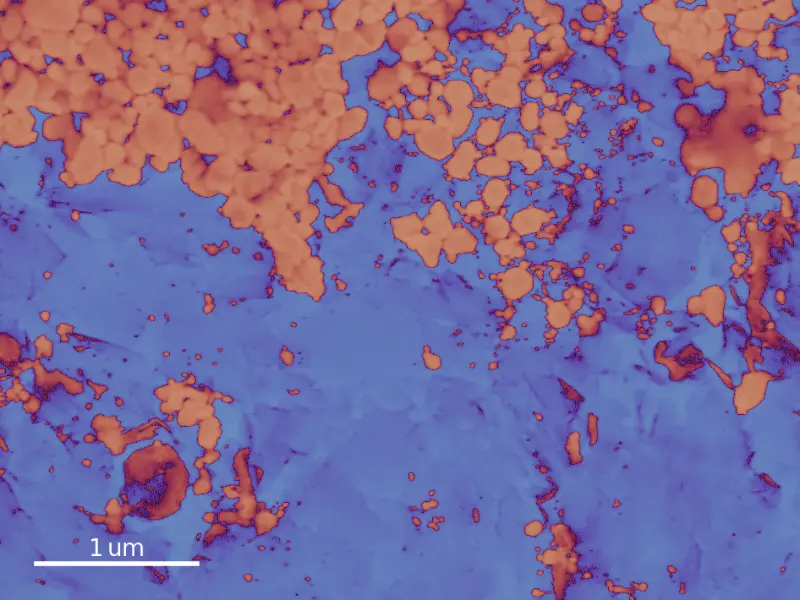
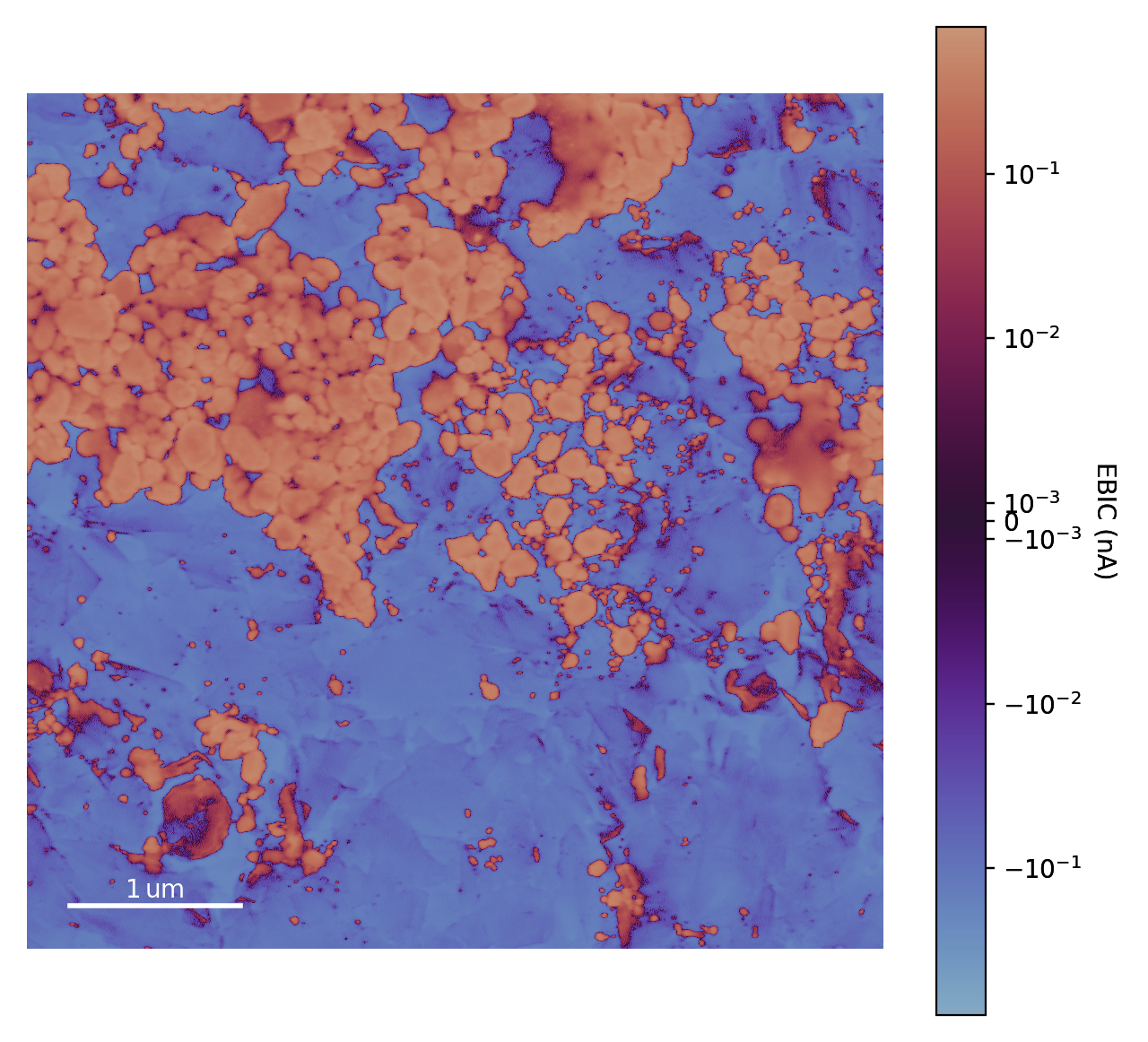
The examples below show a comparison SEand EBAC imaging.
Benefits and Further Reading
- Our partners and nanoprobing specialists Imina Technologies have written many application notes dedicated to EBIC / EBAC and related techniques, https://imina.ch/en/download-center/6-application-notes, https://imina.ch/en/applications
- Ephemeron Labs presents an elegant, succinct introduction to the technique: https://www.ephemeron-labs.com/technique
- A broad review of the technique, with detailed insights on various specialty techniques and quantitative analysis: Leamy, H. J. (1982). "Charge collection scanning electron microscopy". Journal of Applied Physics. 53 (6). https://doi.org/10.1063/1.331667
Latest Scientific Publications
Explore our high-resolution cathodoluminescence tools designed for superior materials characterization.

